facebook rss twitter

Samsung announces start of HBM2 mass production

by Mark Tyson on 22 January 2016, 10:31

Tags: Samsung (005935.KS)

Quick Link: HEXUS.net/qacx3i

Add to My Vault: x

Samsung has officially announced that it has started mass production of second generation high bandwidth memory, or HBM2 for short. The production utilises Samsung's efficient 20nm process technology and advanced HBM chip design. Samsung headlines the new memory chips as being a breakthrough for high performance computing (HPC) tasks but most HEXUS readers will be more interested in HBM2 chip deployment in graphics cards.

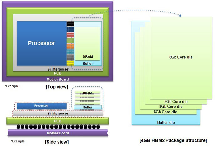
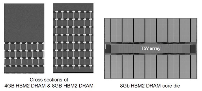
This newly introduced 4GB HBM2 is the latest milestone in Samsung's progress using TSV (Through Silicon Via) DRAM technology. The 4GB HBM2 package is composed of 4x 8Gb core dies fixed atop of a buffer die. Samsung explains that each 8Gb HBM2 die contains over 5,000 TSV holes - that's 36 times more than in an 8Gb TSV DDR4 die - facilitating "a dramatic improvement in data transmission".

Comparisons with HBM1 aren't so stark but the 256GBps of bandwidth offered by the new DRAM package is double what could be achieved with the earlier generation HBM and not to be sniffed at.

Later this year Samsung will start to produce 8GB HBM2 DRAM packages. The firm links these packages directly to the graphics card business, saying that "by specifying 8GB HBM2 DRAM in graphics cards, designers will be able to enjoy a space savings of more than 95 percent, compared to using GDDR5 DRAM, offering more optimal solutions for compact devices that require high-level graphics computing capabilities."


HEXUS Forums :: 9 Comments

Login with Forum Account

Don't have an account? Register today!
Place bets - Team Green or Team Red to implement HMB2 first?
fiver on team red!
Isn't Team Red part of the group that owns HBM? Would be weird if they didn't implement it first :P
9 layers of TSV is an impressive achievement, although I guess that once you've mastered one layer and aligning that, the rest are easy.

Interesting fact - after the wafers are thinned for use in the stack (compare the top and other dies in the 4Hi stack picture) the wafers are bendy: http://1.bp.blogspot.com/-QQFJ2xq-Q_E/UQwBpc965UI/AAAAAAAAACI/2dZpRLZDWWY/s1600/taiko02.jpg which isn't good, so they need to use special transports (or leave the outside unthinned as a rigid exoskeleton).
Well, if the discussions in http://forums.hexus.net/hexus-news/352892-amd-polaris-10-polaris-11-gpus-become-available-mid-2016-a-2.html#post3597275 are even semi-accurate ( ;) ), nvidia don't even have working Pascal silicon yet, and they have no experience releasing consumer products with HBM or on interposers. Historically ATi/AMD have always been earlier proponents of new memory technologies: I'm pretty sure they were ahead of nvidia with GDDR4, GDDR5, and of course HBM. it would be something of a turn-around for nvidia to beat them to the release of HBM2 GPUs; it'd be the first time in more than a decade that they'd be first to exploit a new memory technology…