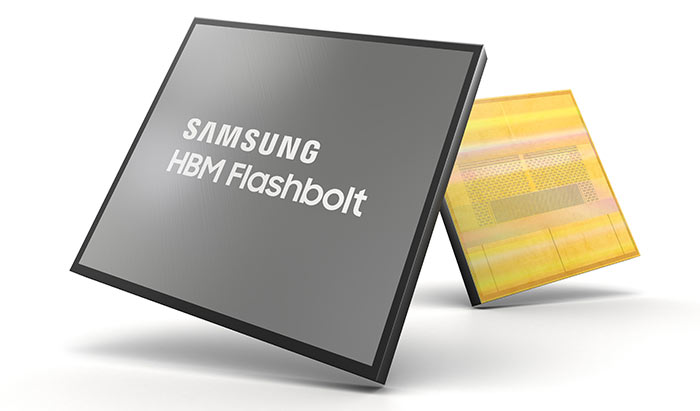
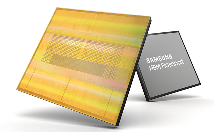
Samsung first announced its Flashbolt 3rd gen HBM2E at Nvidia's GPU Technology Conference (GTC) in San Jose last March. At long last the company has got around announcing expected volume production - H1 this year. Flashbolt memory can facilitate double capacity (16GB) while significant increasing performance and power efficiency - compared to the previous-generation 8GB HBM2 Aquabolt. Samsung thinks Flashbolt will be important to supercomputers, AI-driven data analytics, and state-of-the-art graphics systems.

To recap on the capabilities of Flashbolt, this industry-first HBM2E memory is said to deliver 3.2Gbps per pin, which is a significant 33 per cent faster that previous generation HBM2. Furthermore, an HBM2E 16GB package can deliver 410GB/s data bandwidth. The maximum tested data rate exceeds this base line by some degree. Samsung has achieved transfer speeds of 4.2Gbps, enabling up to a 538GB/s bandwidth per stack in certain future applications. For previous gen comparison, Aquabolt maxed out at 2.4Gbps per pin or 307GB/s per stack.
Of course the capacity increase from Flashbolt will be welcome in high-end applications too. Samsung says that the 16GB capacity is achieved by vertically stacking eight layers of 10nm-class 16Gb DRAM dies on top of a buffer chip. Then the HBM2E package is interconnected in a precise arrangement of more than 40,000 TSV microbumps - with each 16Gb die packing in 5,600 TSV perforations.

With GTC 2020 not very far away (March), perhaps Samsung will make some further announcements at this event - alongside Nvidia. Volume production of Flashbolt memory will begin in the first half of this year but Samsung says it will continue to supply partners with second gen Aquabolt memory for the time being too. SK hynix is also working on HBM2E, which is scheduled for mass production this year.


