Overview
This HEXUS.help guide discusses Intel’s 45nm process technology. What it is, what it provides, and how it benefits the consumer.
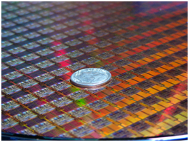
What is a die shrink?
Every once in a while, a processor manufacturer will undergo a die shrink. The shrinking process, popular among semiconductor manufacturers, involves creating near identical circuitry using a more advanced fabrication process.
In simple terms, it literally means making a processor smaller, whilst retaining performance and functionality. By doing so, manufacturing costs are reduced due to more processor dies being manufactured on the same piece of silicon wafer. This in turn will result in increased revenue through greater number of products sold.
What is Intel’s 45nm process technology?
Intel describes its 45nm high-k silicon technology as one of the biggest advancements in fundamental transistor design in 40 years, what makes it so significant? Let’s take a look.
Intel’s hugely popular processor line-up, headed by the Intel Core 2 Duo and Intel Core 2 Quad, have been manufactured on a 65nm process ever since they launched in mid-2006. Now, a little less than two years later, Intel is making a move to a smaller 45nm manufacturing process.
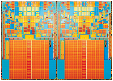
Intel’s 45nm process technology, sometimes referred to as Intel’s high-k metal gate silicon technology, uses new materials, including hafnium-based Circuitry, and packs nearly double the number of transistors into the same silicon space as Intel’s 65nm technology.
To put things into perspective, that’s more than 400 million transistors for dual-core processors and more than 800 million for quad-core. Intel’s 45nm technology provides up to 50 per cent larger L2 cache and superior energy efficiency to its older 65nm predecessor whilst delivering more than a 20 percent improvement in transistor switching speed, and reduces transistor gate leakage by over 10 fold.
What does Intel’s 45nm process mean to the consumer?
We’ve established that Intel’s 45nm process is hugely important to Intel, but how does it affect the consumer?
Well, a die shrink is beneficial to the consumer in numerous ways. It ultimately results in a product with less power consumption, lower heat output, increased performance, and lowered prices. Essentially, a processor that’s far more efficient.
Intel first debuted its 45nm process with its Core 2 Duo T5000/T7000 series of mobile processors, code-named Penryn.
Having launched Penryn in late 2007, Intel’s 45nm-based Core 2 Duo and Core 2 Quad desktop processors, codenamed Wolfdale and Yorkfield respectively, have slowly but surely become readily available.
Wolfdale, Intel’s 45nm-based Core 2 Duo desktop processor, features two processor cores sharing 6 MiB of L2 cache, operating at 2.66 GHz and above. It utilises an FSB of 1333 MHz and includes the SSE4.1 media extensions.
Yorkfield, Intel’s 45nm-based Core 2 Quad desktop processor, features a dual-die quad core design with two unified 6 MiB L2 caches resulting in a total 12 MiB of L2 cache. They also feature a 1333 MHz FSB and were released in late March 2008.
What’s next for Intel’s die size?
In keeping with semiconductor manufacturers’ die-shrinking process, Intel’s 45nm process technology will be superseded with its forthcoming microarchitecture, codenamed Nehalem. Nehalem, however, is for another day, and another HEXUS.help guide.