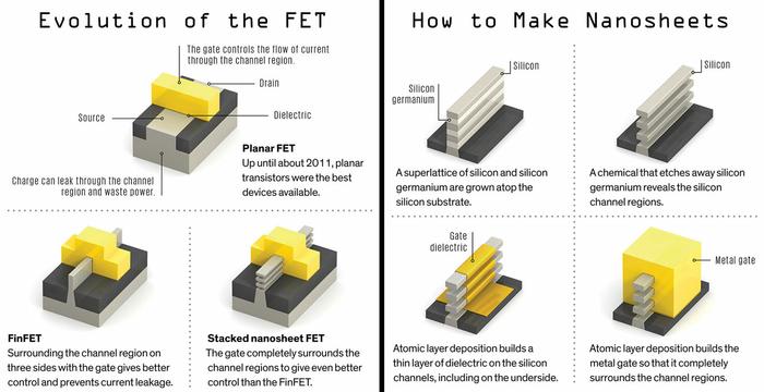
It is expected that today's popular FinFET transistor design will give way to stacked nanosheet transistors in the coming years – for various design and technology reasons. TSMC plans to stick with FinFET for 3nm, but Samsung is bravely / dangerously forging ahead with plans for a transition to nanosheet transistors with its 3nm nodes, reports IEEE Spectrum.
Samsung Electronics vice president, Taejoong Song, presented at the IEEE International Solid-State Circuits Conference earlier this month and outlined some key advantages of nanosheet transistors. "We have used FinFET transistors for about a decade, however at 3nm we are using a gate all around transistor," Song told the virtual audience. Going forward he and his team believe that nanosheet transistors will be a winning design as they provide "high speed, low power, and small area."
Key advantages of these new transistors over FinFET, discovered by Samsung thus far, include:
- Design flexibility, especially in adjusting the 'effective width', or Weff, of the transistor channel
- Excellent potential for next gen SRAM ICs, as minimum voltage needed to switch the state of the cell is significantly reduced
- Potential for greater performance transistors using less power in a smaller area
Diagram from previous IEEE Spectrum article on Nanosheet Transistors
It is worth noting that while the IEEE Spectrum article refers to Samsung's advanced tech as nanosheet transistors, the same tech is variously and interchangeably known as 'multibridge channel MOSFETs' (MBCFET), and 'gate-all-around transistors'. Samsung expects to implement its 3nm MBCFET fabrication technology in 2022.


