Samsung and TSMC have provided updates to their manufacturing process progress today. These South Korean and Taiwanese companies, respectively, are reporting successful steps beyond 7nm - a process which has only just started to yield consumer parts in the last few months.
Samsung completes 5nm EUV development
The headline is an eye opener but 5nm mass production is still some way off. In its update, Samsung said that following on from its first mass produced 7nm output in September last year it has made some significant advancements.
Samsung is "collaborating with customers on 6nm, a customized EUV-based process node, and has already received the product tape-out of its first 6nm chip," according to the official Samsung News blog. That in itself sounds impressive but much of the news post is devoted to the headlining progress in 5nm EUV lithography.
The 5nm FinFET process will provide "up to a 25 percent increase in logic area efficiency with 20 percent lower power consumption or 10 percent higher performance," asserts Samsung. The firm says that 5nm EUV leverages EUV lithography in metal layer patterning and reduces mask layers while providing better fidelity, just like its predecessor. Furthermore, there is a benefit that Samsung can reuse all the 7nm intellectual property (IP) on 5nm, for reduced migration costs and so on.
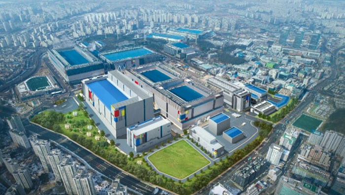
Lastly we hear that Samsung is expanding its EUV production facilities in Hwaseong. This expansion is expected to complete in H2 2019 and deliver a production ramp up from early 2020.
TSMC announces its N6 process
Today TSMC announced that it had started to offer customers an enhanced 6nm process. In an official news blog post TSMC said that the new process, dubbed N6, "provides a significant enhancement of its industry-leading N7 technology and offers customers a highly competitive performance-to-cost advantage as well as fast time-to-market with direct migration from N7-based designs". Processors using the N6 process will benefit from "18 per cent higher logic density over the N7 process."
Like Samsung's process refinements, noted above, TSMC's move will carry allow the reuse of its comprehensive design ecosystem proved with its 7nm process.
For commercial availability, you will have to wait until sometime in 2020 by the sound of it, as in Q1 year TSMC will kick-off its scheduled risk production. Later in 2020 we should find devices benefitting from the "higher performance and cost advantage," over N7 products.
AMD 7nm PlayStation 5 chips at TSMC
Another chipmaking nugget hitting the new wires today comes via Taiwan's DigiTimes. The linked report says that "AMD's 7nm CPU and GPU are expected to be adopted by Sony in its next-generation PlayStation and the processors are estimated to be ready in the third quarter of 2020." That means the next gen Sony console will be ready for Xmas and New Year 2020 to 2021.