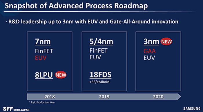
Samsung has confirmed that it has started wafer production on its new 7LPP node. That stands for 7-nanometer Low Power Plus. The process uses extreme ultraviolet (EUV) lithography technology and demonstrates that Samsung's Foundry can follow its roadmap with "a definite path to 3nm".

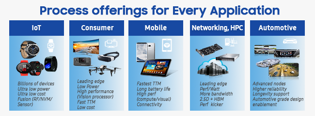
"With the introduction of its EUV process node, Samsung has led a quiet revolution in the semiconductor industry," said Charlie Bae, EVP of the foundry sales and marketing team at Samsung Electronics. Bae went on to say how the UEV process delivers a "fundamental shift in how wafers are manufactured," and will help foundry customers "significantly improve" their mobile and HPC products. More specifically Samsung seems the benefits of the new process pushing the boundaries of 5G, Artificial Intelligence, Enterprise and Hyperscale Data centre, IoT, Automotive, and Networking.

The EUV technology used by Samsung uses 13.5nm wavelength light to expose silicon wafers. This compares very favourably against conventional argon fluoride (ArF) immersion technologies "that are only able to achieve 193nm wavelengths and require expensive multi-patterning mask sets," says Samsung. Furthermore, with EUV a single mask can be made to make a wafer where ArF could need up to four masks for the same job. Tech watchers will also be aware of the other potential benefits of a process shrink, which are delivered here too. Overall, Samsung sees the following benefits with its new 7nm LPP process, compared to its 10nm FinFET predecessor:
- 40 per cent increase in area efficiency,
- with up to 20 per cent higher performance,
- or up to 50 per cent lower power consumption,
- significantly fewer layers,
- better yields.
The initial EUV production has started in Samsung's S3 Fab in Hwaseong, Korea. The technology is expected to step up to 'high-volume' production in 2020 with new EUV capacity expected to be secured.

Samsung is helping industry partners get on board with EUV 7nm by developing tools such as a "unique mask inspection tool that performs early defect detection in EUV masks, allowing those defects to be eliminated early in the manufacturing cycle." It will also work with partners to provide Foundation and Advanced IP, Advanced Packaging, and Services to get them up and running on the new technology.


