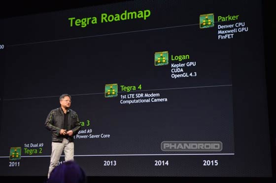
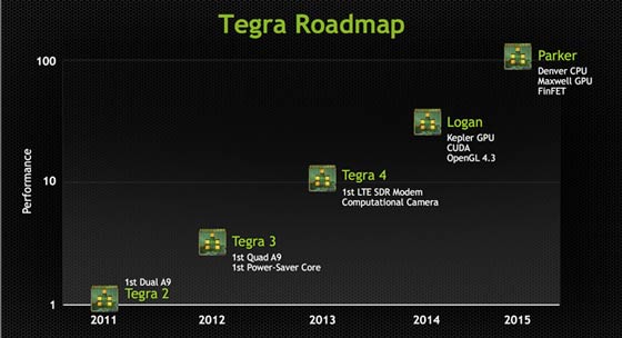
At the GPU Technology Conference (GTC) in San Jose, California yesterday, Nvidia CEO Jen-Hsun Huang fleshed out details of the Tegra SoC roadmap. He told attendees at his keynote speech that the Tegra 5 “Logan” is to include a Kepler-class GPU and will debut this year before full scale production in 2014. The Tegra 6 SoC “Parker” is going to be based upon a 64-bit ARM CPU and Nvidia’s next generation Maxwell GPU. Huang said that the journey from Tegra 2 to Tegra 6 will have brought a 100 times improvement in performance.

Tegra 5 “Logan”
Huang told attendees at GTC that the Tegra 5 is going to be a processor that will allow mobile devices to do “everything a modern computer should do”. Tegra 5 will be the first mobile processor to incorporate a Kepler-class GPU which will be fully CUDA 5 and OpenGL 4.3 compliant “out of the box”. CUDA allows the GPU to be used for many computational tasks other than graphics and image processing.
The Nvidia CEO said that Logan will debut this year before full scale production in early 2014.

Tegra 6 “Parker”
Parker will be the first Tegra SoC to be based upon ARM’s 64-bit Project Denver CPU. This processor is destined to be produced using the 3D finFET process which will have beneficial power consumption and performance effects. The Tegra 6 will also feature Nvidia’s Maxwell GPU which is due to be seen in desktop add-in-cards next year. The Maxwell GPU has a unified virtual memory architecture “All memory will be visible to all the processors” including the compute cores, explained Huang.
When the Tegra 6 Parker SoC is released in 2015 it will achieve 100x the performance of the Tegra 2 according to Huang. If Tegra progress had followed Moore’s Law the processor would have only been about eight times faster but “disruptive technology” had brought about this “quite staggering” rate of innovation.


