


0

VIA and Yamashita Introduce World’s First Lead-free VIA Eden Platform Based Mainboard
|
Tags:
NVIDIA (NASDAQ:NVDA)
Quick Link: HEXUS.net/qacsu
Add to My Vault:
|
|
Taipei, Taiwan and Tokyo, Japan, 21 April 2004 - VIA Technologies, Inc, a leading innovator and developer of silicon chip technologies and PC platform solutions, and Yamashita System, Co. Ltd., a leading supplier of industrial automation systems, today announced the AS-1210, the world’s first lead-free mainboard based on the award winning VIA Eden Platform.
A leading proponent of “Green Computing”, VIA continues to spearhead the drive for environmentally friendly computing by emphasizing power efficiency and ergonomics, and through the early adoption of manufacturing processes that exclude hazardous substances such as lead. VIA’s move to lead-free manufacturing started in 2001 with the introduction of the Enhanced Ball Grid Array (EBGA) package featured on power efficient VIA processors, and the Heat Sink Ball Grid Array (HSBGA) package for its market leading chipsets.
Today, manufacturing of all VIA Eden ESP, Antaur and C3 processors and a wide range of VIA chipsets and companion chips, is lead-free, making it possible to produce totally lead-free motherboards, such as the new AS-1210 from Yamashita System, Co of Japan.
“The transition to ‘green’ manufacturing for VIA has been very smooth and we have been able to ship lead-free processors and chipsets since the end of last year,” said Richard Brown, Vice President of Marketing, VIA Technologies, Inc. “The AS-1210 clearly demonstrates the technology leadership of VIA and Yamashita in being the first to market with a lead-free motherboard that meets the requirements of the international market.”
“Market demands in the embedded space are very dynamic and at Yamashita, we pride ourselves in being able to react quickly to changing customer requirements while continuing to deliver the very best quality of products,” said Shinichi Yanagi, Managing Director of Yamashita Systems, Co, Ltd. “By using the lead-free VIA Eden Platform, we are able to cut back on R&D and validation time, enabling us to be first to market with our products because we practically get the whole platform from VIA.”
Now entering mass production, the AS-1210 Micro-ATX mainboard integrates the fanless VIA Eden ESP processor and the VIA CLE266 chipset with the VIA VT8235 South Bridge and will be on display at Techno-Frontier show from the 21st to the 23rd of April, 2004 in Tokyo at the Makuhari Messe International Exhibition Hall, booth No. 7203. More information on the AS-1210 can be seen on the Yamashita website at:
http://www.misnet.co.jp/prd1210.htm.
VIA’s Lead-Free Manufacturing Initiative
In traditional manufacturing processes, lead is used to attach the chip to the motherboard through tiny solder balls on the underside of the package. With VIA’s lead-free manufacturing technologies, the solder balls now consist of a tin, silver and copper composite.
VIA’s lead-free manufacturing processes will comply with the Restriction of Hazardous Substances (RoHS) and Waste Electrical and Electronic Equipment (WEEE) European Union directives that are helping to speed up the move to environmentally friendly computing. More information on VIA’s lead-free manufacturing can be found on the VIA Green Computing Website: http://www.via.com.tw/en/VInternet/leadfree.jsp
About the VIA Eden ESP Processor
The VIA Eden Platform is based on the ultra low power native x86 VIA Eden ESP processor and a choice of highly integrated and power efficient VIA chipsets and companion chips. Available at speeds ranging from 300MHz to 1GHz and featuring the lead-free EBGA package that helps reduce thermal density, VIA Eden ESP processors measure a mere 35mm x 35mm x 1.5mm, making them suitable for consumer electronics, industrial and commercial devices that require compatibility with PC hardware and software. With Thermal Design Power (TDP) values ranging from 2.5W to a maximum of 7W when running at 1GHz, the VIA Eden ESP processor boasts the world’s lowest power consumption from a native x86 processor.
The VIA Eden ESP processor can be coupled with the highly acclaimed VIA CLE266 chipset, featuring an integrated hardware MPEG-2 decoder, DDR266 SDRAM support, VIA Vinyl™ Audio integrated 6-channel surround sound, high-speed USB2.0 ports, and 10/100 Mbps Fast Ethernet.
For more information on the VIA Eden ESP processor, please visit the VIA Eden ESP processor website at: http://www.via.com.tw/en/Products/eden_esp10000.jsp.
About Yamashita Systems, Co.
Yamashita Systems, Co. Ltd. is a pioneer in industrial automation with the highest standards in the planning, development and manufacture of industrial microcomputer boards. Founded in November 1973, Yamashita has built a strong reputation for excellence in craftsmanship, technical consulting and sales in the industrial PC market and is a strong proponent of environmentally friendly computing and manufacturing practices.
About VIA Technologies, Inc.
VIA Technologies, Inc. (TSE 2388) is the foremost fabless supplier of market-leading core logic chipsets, low power x86 processors, advanced connectivity, multimedia, networking and storage silicon, and complete platform solutions that are driving system innovation in the PC and embedded markets. Headquartered in Taipei, Taiwan, VIA’s global network links the high tech centers of the US, Europe and Asia, and its customer base includes the world’s top OEMs, motherboard vendors and system integrators. http://www.via.com.tw

Related Reading
 5
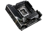
Asus shares its Intel Z690 motherboard guide
5
Asus shares its Intel Z690 motherboard guide
And rivals such as Gigabyte, MSI and EVGA outline their Z690 chipset offerings.
 1
Asus ROG Strix Z690-I Gaming Wi-Fi motherboard images leak
1
Asus ROG Strix Z690-I Gaming Wi-Fi motherboard images leak
Mini-ITX board uses daughterboards to pack in features but maintain its diminutive footprint.
 21
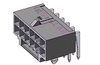
Diagrams of 12VHPWR 600W connectors for GPUs spotted
21
Diagrams of 12VHPWR 600W connectors for GPUs spotted
Power connector is part of the PCIe 5.0 standard and rumoured for the RTX 3090 Ti.


