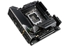
Asus CUSL2
On
with the Specs...
-
Chipset- Intel i815E
-
FSB Speeds- 66-200
-
Multipliers= Auto( should support high celly 2)
-
Dimm Slots = 3
-
PCI Slots = 6
-
ISA Slots = 0
-
AMR Slots = 0
-
CNR Slots = 2
-
AGP Slot = 4x/PRO
-
SB Link = Yes
What's
in the box?
-
1x Asus CUSL2 Mainboard
-
1x UDMA 66/100 Cable
-
1x UDMA 33 Cable
-
1x Serial port lead
-
1x 3 USB thing( erm sorry its a bit vague)
-
1x user Manual
-
2x Driver CDs ( one for Yamaha stuff, one for 815 stuff)
Official
Specs ( the most interesting part of course :)
Processor
Socket 370 for Intel® FCPGA Pentium® III 450MHz~933+MHz processors and
Intel® PPGA CeleronTM 333~566+MHz.
Chipset
-
Intel® 82815 Graphics and AGP Memory Controller Hub (GMCH)
-
Intel® 82801BA Enhanced I/O Controller Hub 2 (ICH2)
-
Intel® 82802AB Firmware Hub (FWH)
-
Support 4x AGP, 4MB AIMM, PC133/PC100 SDRAM, UltraDMA/100 IDE Devices
Super
I/O & USB Hub
-
ITE IT 8703F LPC Chip
-
AU9254 USB Hub
FSB
-
66/100/133 MHz Front Side Bus
System
Memory
-
3x 168-pin DIMM supporting 8MB to 512MB 3.3V PC133/100 SDRAM
-
Maximum 512MB PC133/PC100 non-ECC SDRAM
Expansion
Slots
-
1 x 32-bit AGP Pro/AGP 4X slot
-
6 x 32-bit PCI
-
2x CNR (Communication and Networking Riser)
-
Supports AGP Pro Slot with Universal AGP Connector and additional Power Connectors to Support Highend 3D or Workstation Class Graphics Adapters
VGA
-
AGP Pro/4X/2X/1X Graphics Adapter Compatible
-
Integrated 4X AGP Graphics
IDE
Ports
-
2 x UltraDMA/100/66/33 Bus Master IDE Ports
-
Supports DVD-ROM, CD-ROM, CD-R, CD-RW, and LS-120 Drives
Special
Features
-
Power Loss Restart
-
ASUS JumperFreeTM CPU Throttle
-
STR (Suspend to RAM)
-
SFS (Stepless Frequency Selection)
-
Vcore & VIO Adjustable
Back
Panel I/O Ports
-
2 x USB Ports
-
1 x Serial Ports
-
1 x Parallel Port (ECP, EPP Port)
-
1 x PS/2 Keyboard Port, 1 x PS/2 Mouse Port
-
1 x VGA Port
Onboard
I/O Interface
-
ASUS® iPanel Connectors
-
3 Headers to Support Optional 5 USB Ports
-
24-pin ASUS® Panel
-
SIR/CIR
-
CPU/Power Supply/Chassis Fan
-
ATX Power
-
IDE LED
-
COM2
-
TV/Out/LCD Module Connectors
BIOS
-
Award® 4Mb BIOS with Full ACPI, SM BIOS 2.3, Green, PnP, Trend® ChipAway Virus (TCAV) & Symbios® SCSI BIOS
Industrial
Standard
-
PCI 2.2, USB 1.1
Manageability
-
Wfm 2.0, DMI 2.0, WOL (Wake-on LAN), WOR (Wake-on Ring), Chassis Intrusion, SM Bus
Accessories
-
User's Manual
-
UltraDMA/66 Cable
-
IDE Cable
-
Floppy Cable
-
3-Ports USB Bracket
Board
Size
-
ATX Form Factor with Size : 20.8cm x 30.5cm (8.2" x 12")

Wh00p
on to the review (hurrah finally there)
Before
I start the review of the board, I will go through a bit about why i chose the
i815e( the 'e' bit is important) over the other Via chipsets and intel chipsets.
First of all Via. Before i even heard about the Solano,
the Via 133A chipset was the only decent chipset around, however its
performance was hardly exceptional. It suffered from many AGP problems, and appalling
memory speeds. Second, was the new i820 chipset( well it was quite old by then)
with its MTH issues and RAMBUS-only "features", and coupled with the
extremely high price for Rambus RIMMs, I soon abandoned that idea. Enter the
Solano and Solano2, now known as the i815 and i815E chipsets. After the huge
farce with Rambus, Intel was producing an abundance of 133Mhz bus Pentium 3s,
but nothing for the average user to run them on, apart from Via. Now the Solano
and Solano2 was here Intel could hold their head high again.. or maybe not. The
CUSL2 was one of the first i815E motherboards to hit the market. The major
difference between the 815 and the 815E(apart from the price) is the inclusion
of the ICH2 rather than the ICH. This allows for 2 more USB ports and more
importantly UMDA100 support. The i815 chipset itself is based on Intel's brand
new idea of its ICH(I/O controller hub), a Firmware Hub(FWH)( a 4Mbit place
where firmware is stored) and the GMCH( the Graphics and memory controller hub),
rather than the old North bridge, which comprised the AGP and system memory, and
the South bridge, which constrained pretty much everything else. These two were
connected through the PCI bus. This maximum speed this could manage was
133Mb/sec. This new architecture is called the Intel Hub architecture. Basically
this new feature allows the GMCH and the ICH to "talk" to each other
across a 266Mb/sec link, over the conventional 133Mb/sec PCI bus. The i815
chipset is also very highly integrated. It features on board graphics( based on
the i810 graphics chip, which was OK for normal use, but TERRIBLE for games,
however it can be slightly increased by the inclusion of a 4MB AIMM card into
the AGP slot. AIMM= AGP In-Line Memory Module) and an on-board 6-channel sound.
Also it comes with support for soft-modem/adsl/network as well. These may be
accessed through the 2 CNR slots. These are the brand new version of the completely
useless AMR slots, which no-one ever used( well i think). These allow for
low-cost inclusion of network adapters or modems for example. There are two
versions of the CUSL2.. the original and the CUSL-M, the only difference being
the M variant includes the on-board audio.
Oh
in case your asking why the motherboard is called the CUSL2, is because first
two letters CU, stand for Copper mine, and SL2 is for Solano2. Simple eh!
I'd
never bought an Asus motherboard before, tending to stick to Abit and Soyo.
after the pretty dismal reviews of the SE6( Abit's i815 solution) I decided to
buy the board. When it arrived it came in a pretty crappy blue box, which hardly
impressed me. Opening it up though, i was suitably impressed. The board came
with huge amounts of things, far more than I ever hoped for. first up, the board
itself is not actually that big, but it comfortably fits inside my generic
midi-tower case. After I had some _major_ problems getting the computer running
due to the COMPLETELY EVIL GORB. damn thing was broken. I didn't notice, comp
was booting but kept beeping. Then I had a look in the BIOS. CPU Temp = 110
Degrees.. NOT GOOD! Still got the burn marks on it :( Anyhow when I finally got
it all running fine, the first thing that comes up is the BIOS screen, asking me
to choose which chip I had. It gave me the option of 650 or 866.. quite kind of
it. Anyhow back to the review.. first time I booted up... everything went well.
When windows booted up.. it installed A LOT of new drivers (ICH and the like). I
had just bought the CPU ( from OcUK) and knew it would do 866 just fine. Great i
thought. rebooted and everything was fine. But 866? In this day of 1.4Ghz P4s
that’s just not cutting it. Next I tried 140Mhz FSB. 910Mhz at default
voltage. Thought i should go higher. 145.. great.. 148.. great( only stable @
1.75v though) 150.. had to increase voltage to 1.85v, but YES a FULL 50%
OVERCLOCK! In fact the CPU could just about boot into windows at 1001Mhz , but
sadly it crashed. Picking up an Articooler, and some Artic silver.. this WILL
hit a Ghz! I have to say one thing about stability: its been completely
top-notch. Only had a few crashes... mainly due to the Voodoo3 not over clocking
high enough =).
This
board is not entirely perfect, but nothing that cant really be fixed. A new BIOS
comes out every week or so, adding new features, and increasing performance. The
biggest flaw is the problems with Intel’s ATA drivers. If you install then,
then for some bizarre reason the performance seems to go down. In order
to fix this all you do is uninstall it , and reinstall it. Pretty simple,
but still a bother. Also there is a small bug( which I will explain later) which
makes the memory performance decrease after 140mhz Bus.
Benchmarks!


Memory
Problems
Another
major thing I admire about this motherboard is the huge community( mainly based
at www.cusl2.com) which provide help with the board. After many complains about
the decreasing performance, one user found a way to get around it. This involved
using the program WPCREDIT. A program by H-oda, the author of WCPUID. This
programs allows a user to directly configure registers on the motherboard. When
he was looking he found that after 140Mhz, it enabled a few options in order to stabilize
the computers, but slightly decrease the memory performance. By simply chancing
these, the memory performance gets back to normal levels. Here is an example of
my computers, taken at ,140Mhz FSB, and 145Mhz FSB, before the tweak.
Here
are the pictures of 145Mhz tweaked, and my normal running speed of 148Mhz, when
tweaked.( The highest speed where I can run 2-2-2 with my RAM). As you can see,
quite a healthy performance increase! As you can see in the final image, its on
par with the 200Mhz bus of the Athlon, and completely blitzes past the
P3+RAMBUS!

Conclusion.

Pros
-
Fast
-
Stable ( I’ve seen these things hit 170+Mhz FSB and work fine)
-
UDMA100
-
7 USB Ports
Cons
-
Cost
-
Integrated video is POOR!
-
Bizarre memory bug
-
Bizarre ATA Bug
Conclusion