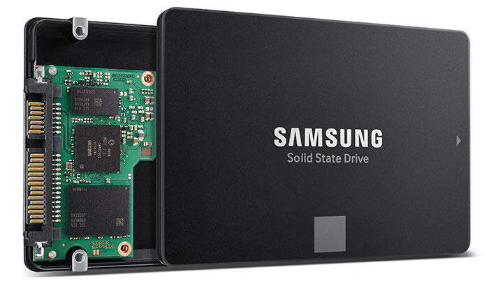
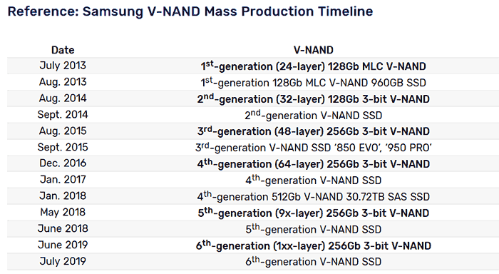
Samsung has announced that it has started mass producing a new line of 256GB SATA SSDs. While hardly inspiring in terms of capacity and interface technology, inside these SSDs you will find the industry's first 100+ layer single-tier 3D NAND design for exceptional performance, efficiency, and a 20 per cent improvement in manufacturing productivity - which should mean keener pricing.
Samsung's sixth-generation V-NAND uses a unique 'channel hole etching' technology to add around 40 per cent more cells to the previous 9x-layer single-stack structure. "This is achieved by building an electrically conductive mold stack comprised of 136 layers, then vertically piercing cylindrical holes from top to bottom, creating uniform 3D charge trap flash (CTF) cells," explains the South Korean tech giant.

With the increased height of the mould stack, Samsung intorduced a new speed-optimized circuit design that allows it to achieve the fastest data transfer speed, at below 450 microseconds (μs) for write operations and below 45μs for reads. The changes result in a >10 per cent improvement in performance, and a reduction in power consumption of >15 per cent. Going forward this technique will be able to facilitate next-generation V-NAND solutions with over 300 layers "simply by mounting three of the current stacks, without compromising chip performance or reliability," says Samsung.
Samsung intends to expand the use of its 3D V-NAND from the consumer space into areas like next-generation mobile devices, the automotive market, and enterprise servers. It has plans to follow up today's announcement with 512Gb three-bit V-NAND SSD and eUFS storage devices in H2 this year.


