facebook rss twitter

HBM2 memory wafer shown off by SK hynix

by Mark Tyson on 20 March 2015, 11:50

Tags: SK hynix, AMD (NYSE:AMD), NVIDIA (NASDAQ:NVDA)

Quick Link: HEXUS.net/qacp5f

Add to My Vault: x

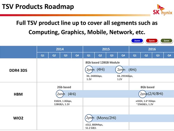
SK Hynix has been showing off HBM2, the next generation of its high bandwidth memory. The first generation HBM1 is expected to premiere on AMD Radeon 300 series graphics cards this summer. The second generation high bandwidth memory from SK Hynix will offer double the density and double the bandwidth of the first generation memory chips. It has been earmarked by Nvidia to form an important component on its Pascal GPU graphics cards in 2016.

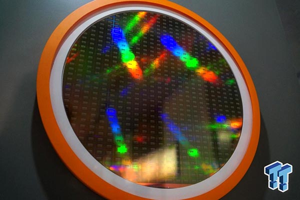
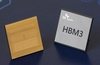
As reported by Tweaktown, which took some pictures of an HBM2 wafer at the SK Hynix stand during the GPU Technology Conference this week (as above), the first and second generation HBM chips compare as follows:


HBM1

HBM2

Bandwidth per stack

128GB/s

256GB/s

Chip density

1Gb

2Gb

Voltage

1.2V

1.2V


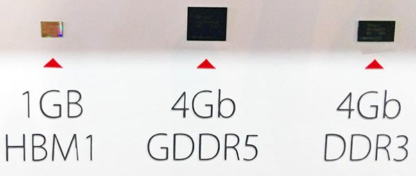
The greater density on offer with the HBM2 memory architecture will enable graphics cards with up to 32GB of RAM. The stacking of the memory chips using Trough Silicon VIA (TSV) technology enables HBM (1&2) memory chips to be much smaller. Fudzilla published a picture showing how much smaller 1GB of HBM1 memory is compared to 4Gb of GDDR5 or 4Gb of DDR3 RAM, see below.

AMD is set to gain a significant performance bonus from the adoption of HBM1 in its available graphics cards, it has got perhaps six months or more before Nvidia can strike back. While Nvidia may have already signalled it will skip straight to HBM2, by the 2016 launch of Pascal AMD may update its graphics card range to include this second generation HBM too.


HEXUS Forums :: 15 Comments

Login with Forum Account

Don't have an account? Register today!
Jesus AMD might really pay for its tardiness in bringing the 300 series to market. If they only have 6 months on Nvidia before they release cards with double the memory bandwidth, doesn't really bode well for AMD.
Nobull
Jesus AMD might really pay for its tardiness in bringing the 300 series to market. If they only have 6 months on Nvidia before they release cards with double the memory bandwidth, doesn't really bode well for AMD.

I have a feeling only 4k+ resolutions are really going to see the benefit of the extra bandwidth anyway. I doubt this is going to sway the market one way or the other yet.
Nobull
Jesus AMD might really pay for its tardiness in bringing the 300 series to market. If they only have 6 months on Nvidia before they release cards with double the memory bandwidth, doesn't really bode well for AMD.
You're right, but I don't see how AMD could do anything else, delaying the 300 series to put the newer memory on just makes it worse
Why is the HBM chip “1GB” where the DDR is “4Gb”?
Nobull
Jesus AMD might really pay for its tardiness in bringing the 300 series to market. If they only have 6 months on Nvidia before they release cards with double the memory bandwidth, doesn't really bode well for AMD.

Depends what they're targeting with it. For gaming, I can't see them needing that much bandwidth: R9 300 is going to have almost twice the bandwidth currently available to Titan X; if Pascal goes for a 4-stack HBM2 arrangement it'd have 4x as much. I don't think gaming graphics are bandwidth limited at the moment: the R9 285 was a great example of getting better performance from less bandwidth by using intelligent texture compression and other tricks. So while the headline bandwidth figure would undoubtedly look impressive, it would largely be wasted for gaming. And while I'd be tempted to suggest it's aimed at compute, nvidia haven't exactly been letting their recent chips stretch their compute legs. Perhaps the reason GM200 is so compute limited is because NV know they need better bandwidth - only time will tell on that one.

Another reason to wait for HBM2 could be the increased density: a 2-stack HBM2 arrangement would give similar framebuffer and bandwidth to AMD's 4-stack HBM1 set-up, but with less complexity/traces/controllers. That saved die space could go into more shaders/cache/etc.

There's a lot of conjecture involved, but I honestly don't believe that nvidia are going to come up, within the next year, with a GPU that needs > 1TB/s memory bandwidth…

EDIT for crosspost:
DDY
Why is the HBM chip “1GB” where the DDR is “4Gb”?

Erm … because it is? ;) Single memory dies tend to have their capacity quoted in gigabits. HBM is a stack of 4 2Gb dies, making a cube with 8Gb capacity. I assume they use 1GB to differentiate between a stack and a single die….