A couple of months ago we heard rumours that AMD had secured priority access to SK hynix's HBM2 chip output. The news sources explained that AMD had worked closely with SK hynix on HBM(2) development and the pair of companies has a long established relationship. Furthermore AMD was expected to strive to capture "as much of the initial production capacity as possible," which could have derailed Nvidia's Pascal GPU launch proper.

In a report published earlier today, Business Korea said that both SK hynix and Samsung Electronics are planning to mass produce second-gen High Bandwidth Memory (HBM) for Nvidia's Pascal GPU. Production will start in Q1 2016 following the pilot production and reliability tests expected to complete later this year.

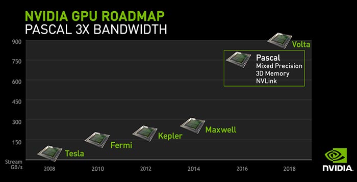
While we know that Nvidia will pair up its Pascal GPU with HBM2 (called 3D memory in its roadmap slide), we don't have any roadmap from AMD indicating what it plans to do with the second generation of this high bandwidth memory. HBM2 offers significant enhancements over the first generation including higher density, higher performance, and lower power usage. More specifically, HBM2 is said to offer twice the bandwidth of HBM and offer a fourfold leap in density, with a maximum chip capacity of 32Gb compared to the 8Gb possible with HBM.

In addition to the HBM2 bandwidth boost, Nvidia says it will enhance the performance of Pascal GPUs with NVLink. This interconnect technology is said to allow data sharing "at rates 5 to 12 times faster than the traditional PCIe Gen3 interconnect".
The first shipments of HBM2 are said to be destined for use with GPUs, like Pascal, and also for servers, supercomputers, networks, and high-performance PCs. It is expected that HBM equipped graphics cards will be 'mainstream' by 2018.


