Can we get that in writing?
In a surprisingly candid interview, NVIDIA's Jen-Hsun Huang has explained some of the problems that led to the delay of the company's latest graphics cards.
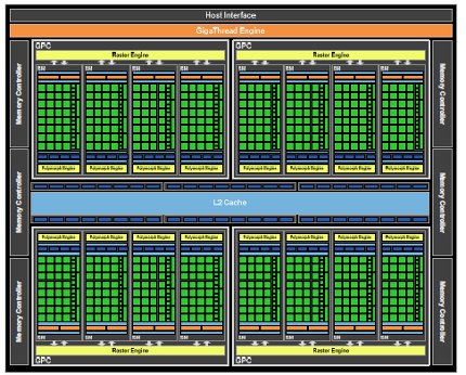
Speaking to journalists - and captured on video by Golem.de - Huang explained how the company discovered that designs on paper don't always accord with what's possible in reality. The issue arose in the way that the Fermi architecture is broken down into multiple Streaming Multiprocessor (SM) clusters that are linked to each other via a series of interconnects.

Huang explained that these interconnects are like the fibres in a piece of fabric - densely packed and tightly layered. On paper, this would allow incredibly fast communication between each of the processing cores and any other part of the chip. However, things didn't quite go to plan.
When the first samples were received back from TSMC, all of the SMs seemed to be working normally - but none of them were able to communicate with each other. Apparently the interconnect was so dense that signals were interfering with each other, completely breaking any connections. This led to something akin to a traffic jam where no information was able to pass across the chip.

Huang described it as "a major breakdown between the models, the tools and reality". The problem arose because the engineers dealing with the physics and the engineers dealing with the architecture belonged to separate groups. While the problem itself wasn't hard to solve, neither group was assigned responsibility for it by the management, meaning that it was never addressed. The result was a broken chip that had to be redesigned, causing the delayed launch of the first Fermi-based graphics-cards.
This was a simple confession, but it's refreshing to see a company openly admit its mistakes - especially on a managerial level - and hopefully learn from them going forwards.


