As promised, Nvidia CEO Jensen Huang delivered his GTC digital keynote today. If you want to digest the whole caboodle, the 'Kitchen Keynote' has been split into eight bite sized chunks on the Nvidia YouTube channel, and here is the playlist. Before we go on, I'll state now that there were no great reveals for consumers - i.e specific news on the GeForce line - but it wasn't really expected and there were still some juicy titbits including, or course, the Ampere architecture reveal.
After an introductory video which began thanking all the essential workers who are keeping the world running during the widespread lockdown (sometimes with help from Nvidia tech), the next video is pretty interesting for PC gamers and enthusiasts. Embedded directly below you will see a video which addresses RTX graphics technology, and while it isn't really news, it is good to see DLSS 2.0 discussed and demonstrated by the Nvidia CEO.
Later in the video embedded above, there is a demo of a fully playable physics-based game which uses both raytracing and AI technology. The Nvidia Omniverse platform, 9mins 45sec in, enables interactive real-time photorealistic environments on a single Quadro RTX 8000 GPU.
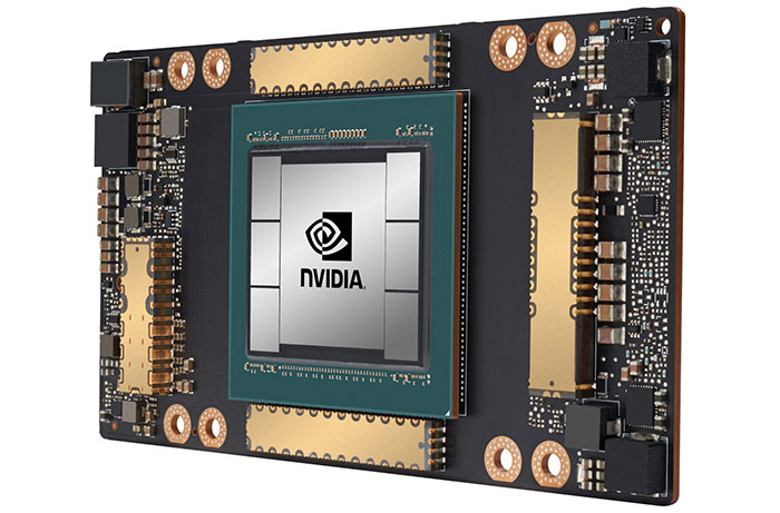
Nvidia Ampere A100 GPU
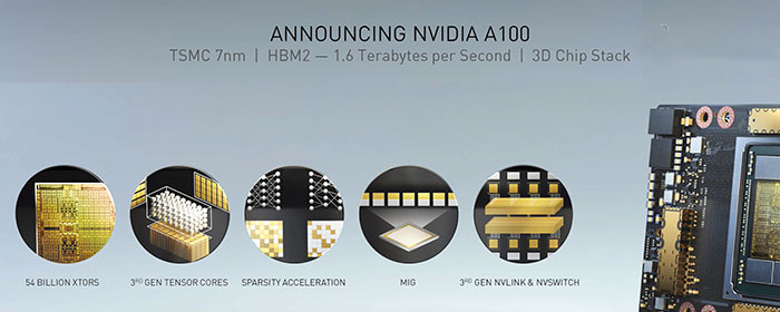
The new A100 GPU is built on the Ampere architecture, claimed to offer the largest generational leap in GPU performance to date. It is the power behind the new DGX A100 AI system which can deliver 5 Petaflops of performance (the system features eight A100 GPUs . Nvidia has built the A100 is also built for data analytics, scientific computing and cloud graphics.
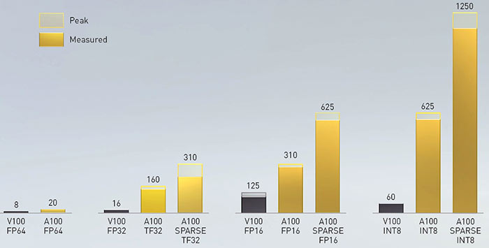
"Nvidia A100 GPU is a 20x AI performance leap and an end-to-end machine learning accelerator — from data analytics to training to inference," claimed Jensen Huang. "For the first time, scale-up and scale-out workloads can be accelerated on one platform. Nvidia A100 will simultaneously boost throughput and drive down the cost of data centres."
Tech specs of the A100 GPU include the following:
- Built on TSMC 7nm with 3D stacking
- Contains 54bn transistors (12nm GV100 GPUs contained 21bn transistors)
- 3rd Gen Tensor cores
- MIG
- 3rd gen NVLink and NVSwitch
- HBM2 1.6TB/s memory
Nvidia DGX A100
The $199,000 DGX A100 packs in eight of the new Nvidia A100 Tensor Core GPUs, providing 320GB of memory for training the largest AI datasets, and the latest high-speed Nvidia Mellanox HDR 200Gbps interconnects. This 5 Petaflop system can be partitioned to act as 56 instances (MIG - multi instance GPU). Alternatively it can work as a combined, single, fully integrated, software-defined platform - "the world's largest GPU".
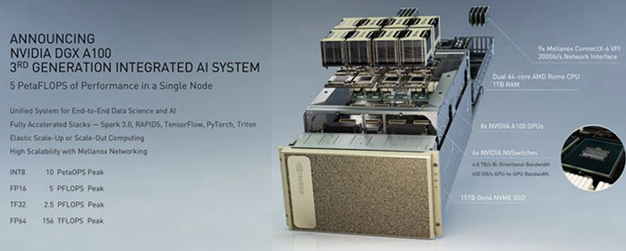
With dual 64-core AMD Rome CPUs
Other announcements from Nvidia today
In other green team news, Nvidia took the wraps off its two EGX Edge AI platform products: EGX A100, the first edge AI product based on NVIDIA Ampere architecture, for larger commercial off-the-shelf servers; and the tiny EGX Jetson Xavier NX for micro-edge servers. It highlighted the Nvidia Mellanox ConnectX-6 Lx SmartNIC, a highly secure and efficient 25/50 gigabit per second (Gb/s) Ethernet smart network interface controller. And it talked about application frameworks for AI computing, its collaboration with BMW in robotics, and partnerships with bio-tech companies looking into problems like Covid-19.
Rumours point to GeForce RTX 3000 graphics cards, based upon Ampere GPU technology, being launched in time for the release of Cyberpunk 2077 in September.