Most PC enthusiasts are excited about the possibilities of AMD's upcoming Zen processor family. AMD is promising to "drive competitive performance" with Zen, with 40 per cent greater instruction-per-clock-cycle throughput via the use of simultaneous hyperthreading. That's with the first generation Zen cores, developed under the watchful eye of legendary CPU architect Jim Keller. While we wait for more official information such as slides and charts it is interesting to see what can be learned from the incidental morsels, such as this preliminary Zen block diagram devised from an AMD software patch.
3DCenter.org has published an AMD Zen block diagram "with little speculation". The diagram was drawn up from a software patch published by an AMD Technical Staff member called Venkataramanan Kumar. The software patch, which "enables -march=znver1 (AMD family 17h Zen processor)," apparently contained enough information to allow someone, with a certain amount of processor design knowledge, to draft a block diagram.
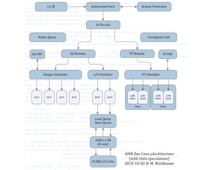
The preliminary block diagram, above, shows that AMD's first generation Zen processors will have; four instruction decoders, four Integer units (ALUs), two address units (AGUs) and four floating-point units (FP) at 128 bit wide. Compared to Bulldozer and Steamroller, Zen will have double the execution units and quadruple floating point units. SMT, similar to Intel Hyperthreading, will be enabled by Zen. The cache sizes are speculation, just to complete the diagram. Further speculation is that the clock speeds that Zen will run at will be between 3.5 to 4.0GHz – even though it will be manufactured at 14 or 16nm.
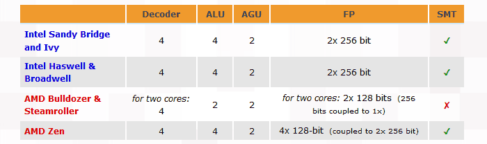
3DCenter processor architecture comparison