


Introduction
In a sign of the times, Nvidia boss, Jen-Hsun Huang, took the wraps off the all-new GeForce RTX 30-series graphics in none other than his kitchen. Based on the Ampere architecture that first debuted in the datacentre space with the A100 GPU, Nvidia reckons it has doubled the performance from the last generation. Lofty claims indeed.
GeForce 30-series is initially represented by the premium RTX 3070, RTX 3080, and RTX 3090. The launch is staggered such that the RTX 3080 is available from today, the champion RTX 3090 on September 24, and the RTX 3070 on October 15. So let's dig further into what Ampere is, how it's manifested in the RTX 3080, and then evaluate the validity of Nvidia's bombast performance claims.
Ampere Architecture
Ampere is an evolution of the Turing architecture powering 20-series and 16-series cards. It makes most sense to examine it in the fullest form and then focus on where Nvidia has made improvements over previous generations.
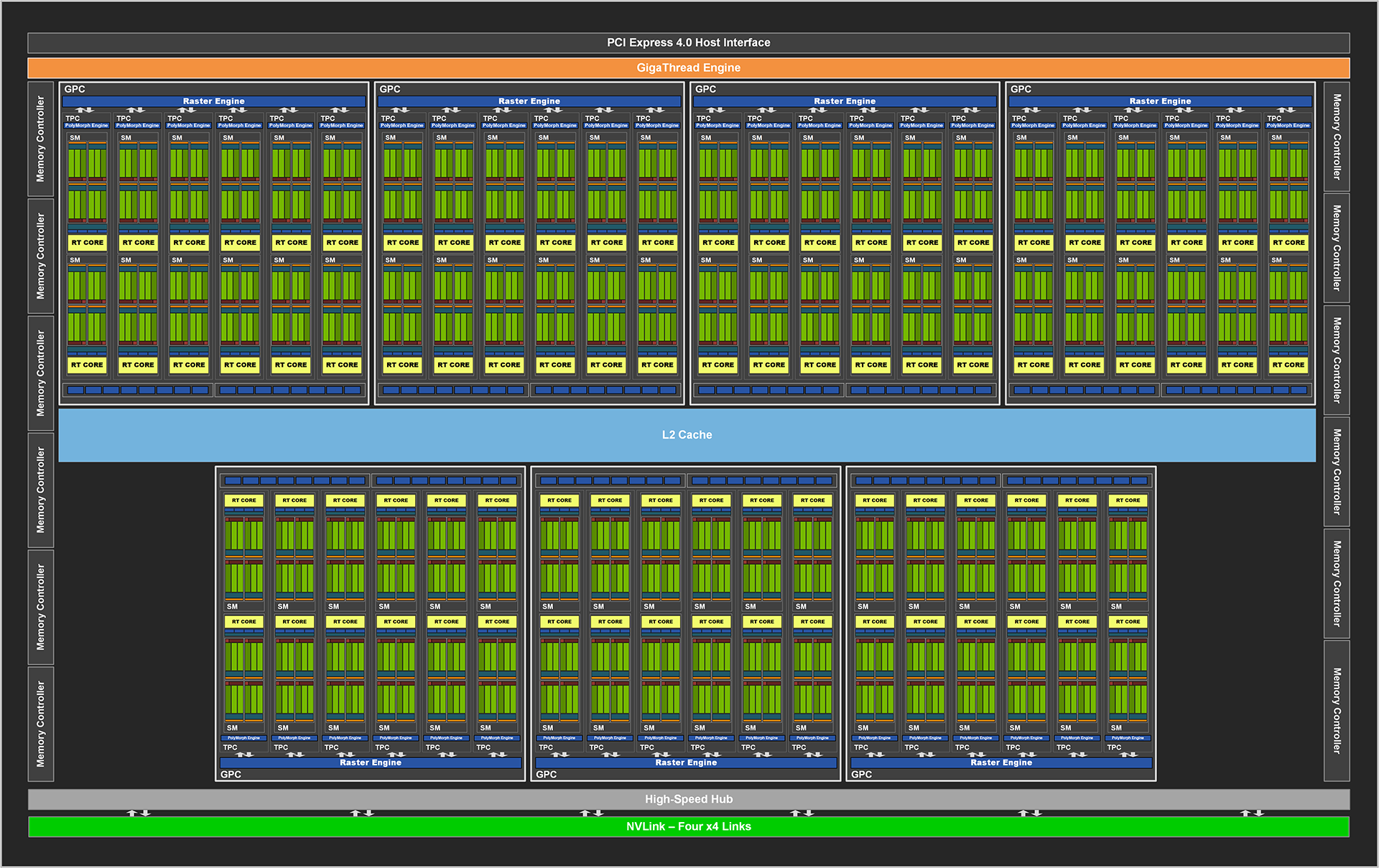
Here is the usual high-level block diagram of the full gaming version of Ampere. Known as GA102, it's a beast of a chip, comprising 28.3bn transistors on a 628.3mm² die manufactured on Samsung's 8nm custom process. The decision not to go with TSMC's 7nm is curious given Nvidia's long-standing relationship with the foundry, but Samsung's leading process has a similar transistor density as TSMC's popular 7nm, so the resultant GPUs would have been of similar size in any case.
Nvidia puts these transistors to work by cramming in more of just about everything that matters for a consumer GPU. The full GA102 die has 10,752 cores, 84 RT cores, 336 Tensor cores, more cache, more memory bandwidth, and PCIe 4.0 connectivity. Yet such a chip doesn't exist. Though RTX 3090 and RTX 3080 are known to use GA102, neither use its complete capability, leaving adequate room for a fully-enabled RTX Titan GPU down the line.
Zooming into the GA102 silicon reveals Nvidia houses 84 streaming multiprocessors (SMs) bunched into groups of 12 within a graphics processing cluster (GPC). It's these SMs, like previous generations, where the bulk of the work is done. Nvidia strives to improve the throughput and efficiency of each SM compared to its immediate predecessor whilst fitting more into the overall design by adopting a smaller manufacturing process. Ampere succeeds on both fronts.
Bulking up the SM and Disconnecting the ROP
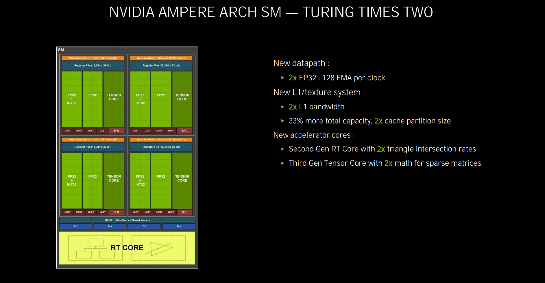
Focussing on rasterisation first, you may recall that last-generation Turing had 64 FP32 cores, also known as Cuda cores, per SM, or exactly half that of the Pascal architecture that preceded it. Nvidia chose instead to imbue the SM with a dedicated datapath for integer operations. The reason for this concurrent FP-and-INT execution lay with how modern games use each type - 36 INTs for every 100 FPs - and thus having a dedicated INT datapath frees up the FP32 cores to focus on what they are best at - floating-point calculations. In Pascal, for example, every time an integer instruction is run the dual-purpose FP32 cores can't do anything else - it is either floats or integers.
Ampere does things differently in the SM. Now, like Turing, there are 64 dedicated FP32 cores, split into four partitions of 16. The big change is that the second datapath, seen to the left in the picture, is not restricted to just INT work. It can also run FP on an as-needed basis. It's important to understand that this second datapath runs either INT or FP, and not both at the same time. This new arrangement actually means each SM has 64 FP32 Cuda cores and a further 64 that can run FP32 or INT.
The upshot is that each Ampere SM has exactly double the FP32 capability of Turing, and this is why you see such startling TFLOPS numbers when perusing the specs. We have established that games don't run FP32 all the time; there's real need for INT processing, so whilst an Ampere-based card might have double the TFLOPS of a leading Turing, it won't be twice as fast. Peak FLOP rate is akin to evaluating a car's performance on engine horsepower alone; it's important, of course, but not the only factor that matters.
Having more grunt in each SM requires the cache levels to be boosted, too. Compared to Turing, Ampere doubles L1 data cache to 128KB and also doubles the shared memory bandwidth to 128 bytes per clock. Feed the beast... and all that.
In another move that speaks to efficiency, Nvidia moves the render outputs (ROPs) from being tied to the L2 cache and memory controller to inside the GPC, at a rate of 16 per cluster. This favourable disconnect means Ampere can increase the number of ROPs relative to the memory interface. As an example, the Turing generation had a maximum 96 ROPs from a 384-bit interface. That's now increased to 112 (7x16) for the same width. Handy for anti-aliasing work.
Last but not least, those interested in double-precision capabilities (FP64) of consumer Ampere need to know there are two dedicated FP64 cores per SM, or exactly 1/64th of FP32. The ratio also defines FP64 performance on a GPU-by-GPU basis, so if a card has, say, 30 TFLOPS of FP32 it will have 469 GFLOPS of FP64.
Removing RT Bottlenecks and Improving Motion Blur
Turing's chief advances centre on introducing dedicated processing blocks for raytracing and neural networks (Tensor cores, DLSS). Ampere, naturally, improves upon them in a few ways. Let's take the RT (raytracing) cores first.
As before, Nvidia invests silicon space into fixed-function RT blocks that take this specific load off the SM units. It's the RT core's job to calculate which light rays need to be drawn by doing bounding volume hierarchy (BVH) and triangle intersection tests. The result is either a hit or a miss, and if it is the former, it's sent back to the SM unit to do its thing. In the meantime, the SM unit continues its usual rasterisation operations.
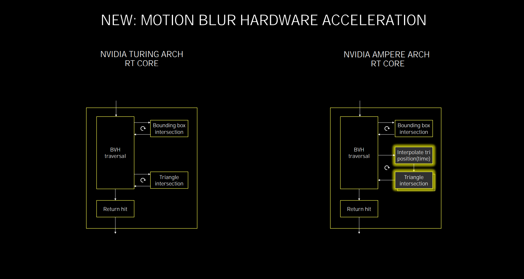
Ampere's RT core works in the same fundamental way as Turing's, but adds two important features for improved performance. The first is the presence of a second unit for conducting the triangle intersection tests, as shown on the bottom right. According to Nvidia, Turing's RT core typically had really solid bounding box intersection rates but the triangle intersection rates, at the end of the flow, before being sent back to the SM, oftentimes presented a bottleneck that slowed the whole process down. Literally doubling this led to greater RT efficiency. Put simply, for the same RT workload, on the same number of cores, Ampere ought to be faster than Turing.
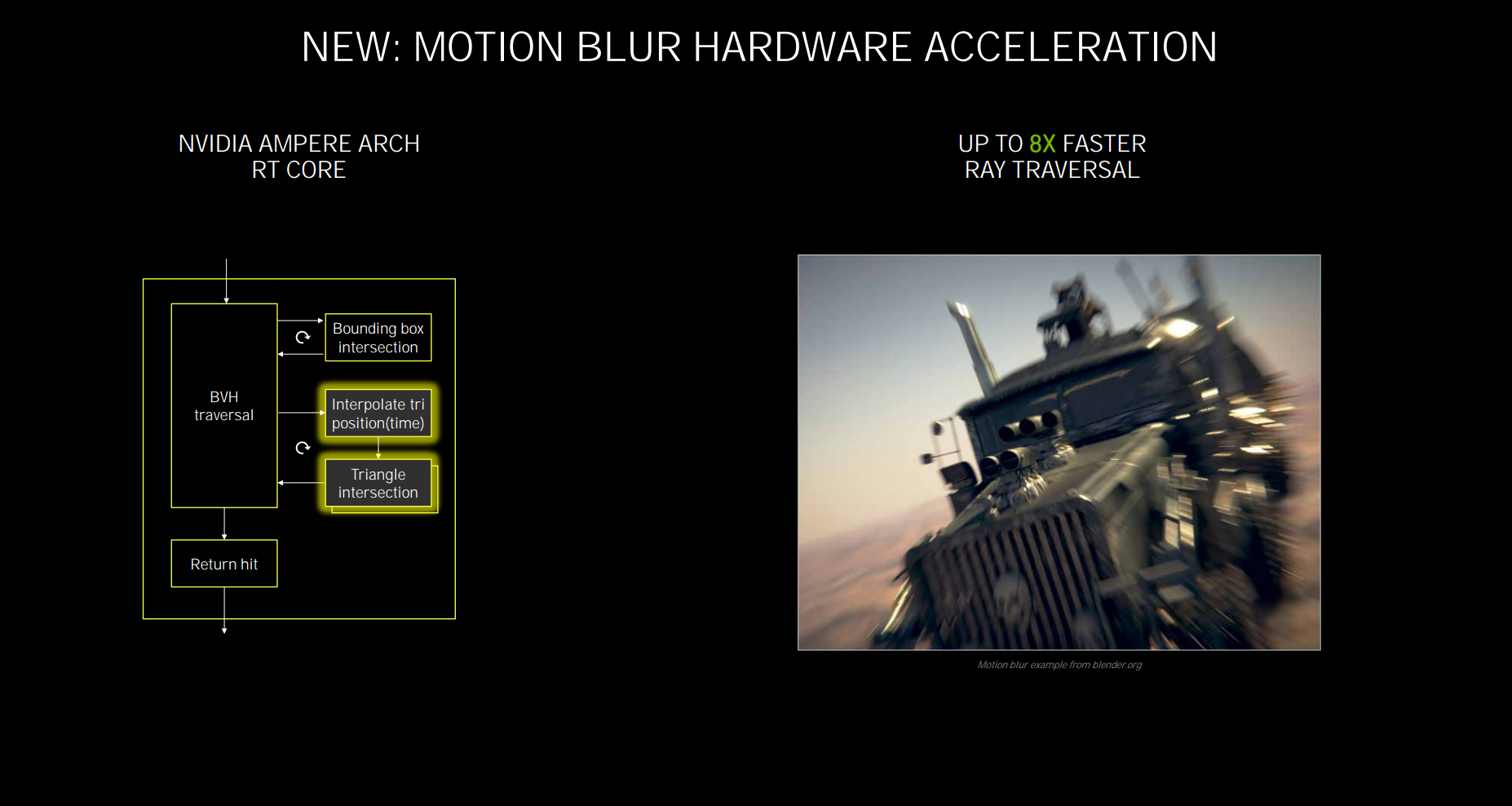
Note the box above? Triangle interpolation position. It's a new feature implemented to accelerate raytracing for motion blur. Put simply, calculating the ray/triangle intersection rate on a regular scene is relatively straightforward - the ray either hits the triangle or it doesn't - yet adding motion blur into the mix makes it more complicated as the RT core is trying to calculate intersections temporally. In other words, for accurate RT lighting on motion blur scenes, the hardware needs to understand that every ray exists at a different point in time. This is where this bit of hardware comes in, and Nvidia says it offers up to 8x the ray traversal of Turing in this corner-case feature.


