


Turing - the new SM unit
Nvidia's GeForce business has been on a good run of late. So good, in fact, that the GTX 10-series, based on the Pascal microarchitecture, has been making hay for over two years. And why not, because the Pascal-based GPUs haven't had really serious competition from rival AMD in all that time.
Yet Nvidia also knows it cannot rest on its laurels forever. The graphics business is an ever-evolving beast, and what GPU hardware architects put into their cutting-edge designs has ramification for present and future games engines. To that end, Nvidia announced the brand-spanking-new RTX 20-series GPUs during Gamescom last month.
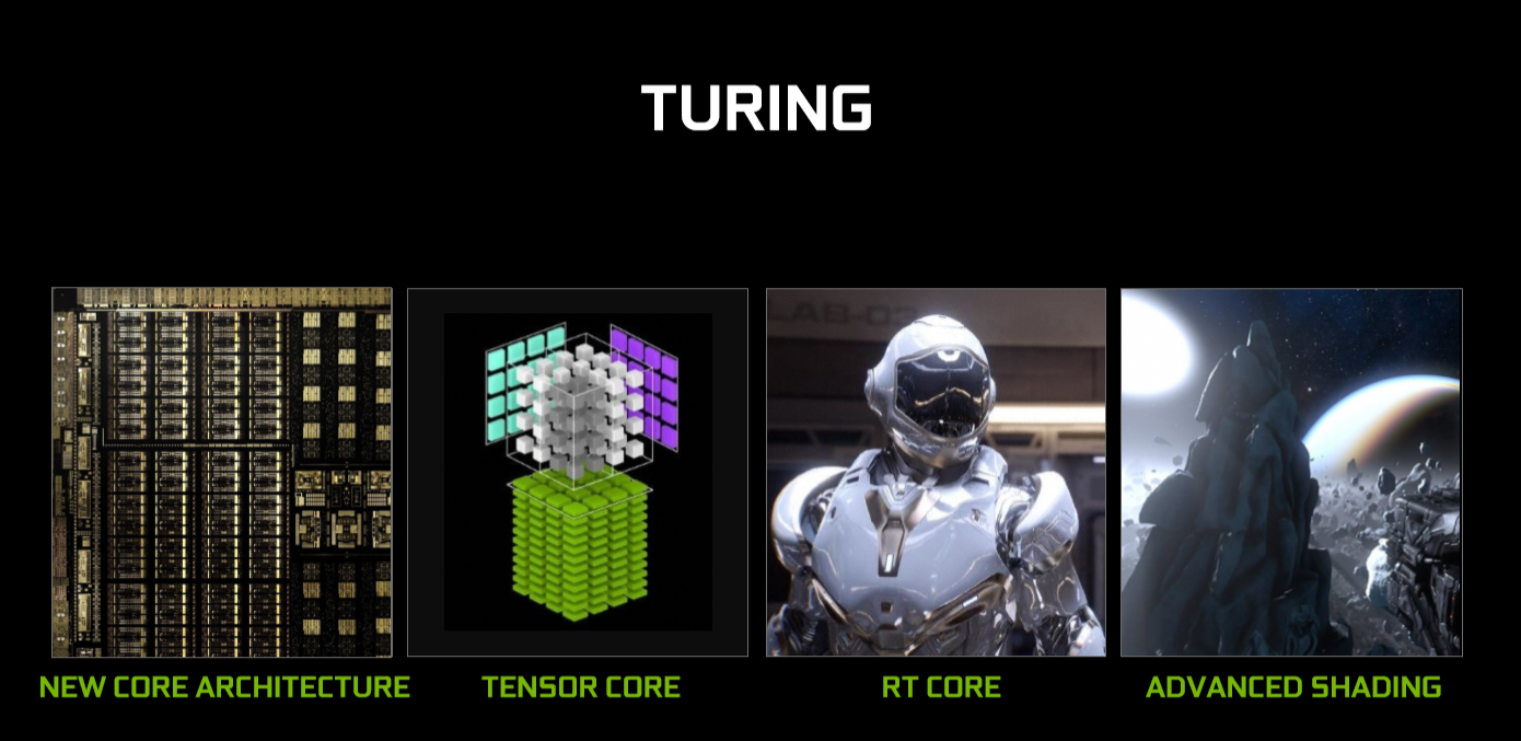
Since then, various titbits have either been divulged officially or leaked out. We already know that RTX cards, hewn from the Turing microarchitecture, improve upon incumbent Pascal in a number of ways, including more, efficient shader cores, new-fangled GDDR6 memory, Tensor cores for hardware-accelerated compute used in deep learning, and a number of RT cores for real-time ray tracing speed-ups.
Turing is in many ways an iterative design that harnesses what's good about the mainly workstation- and server-orientated Volta architecture and adds to it with explicit hardware support for ray tracing. There's plenty going on under the hood, of course, so it's worth paying closer attention to the microarchitecture that will be powering the next slew of GeForce gaming cards.
This article focusses on explaining the new architecture powering Turing-based cards and then turns attention towards the real-world implementation of the GeForce RTX 2080 Ti and GeForce RTX 2080. The full performance review, per Nvidia's NDA, is set for a later date.
New Core Architecture
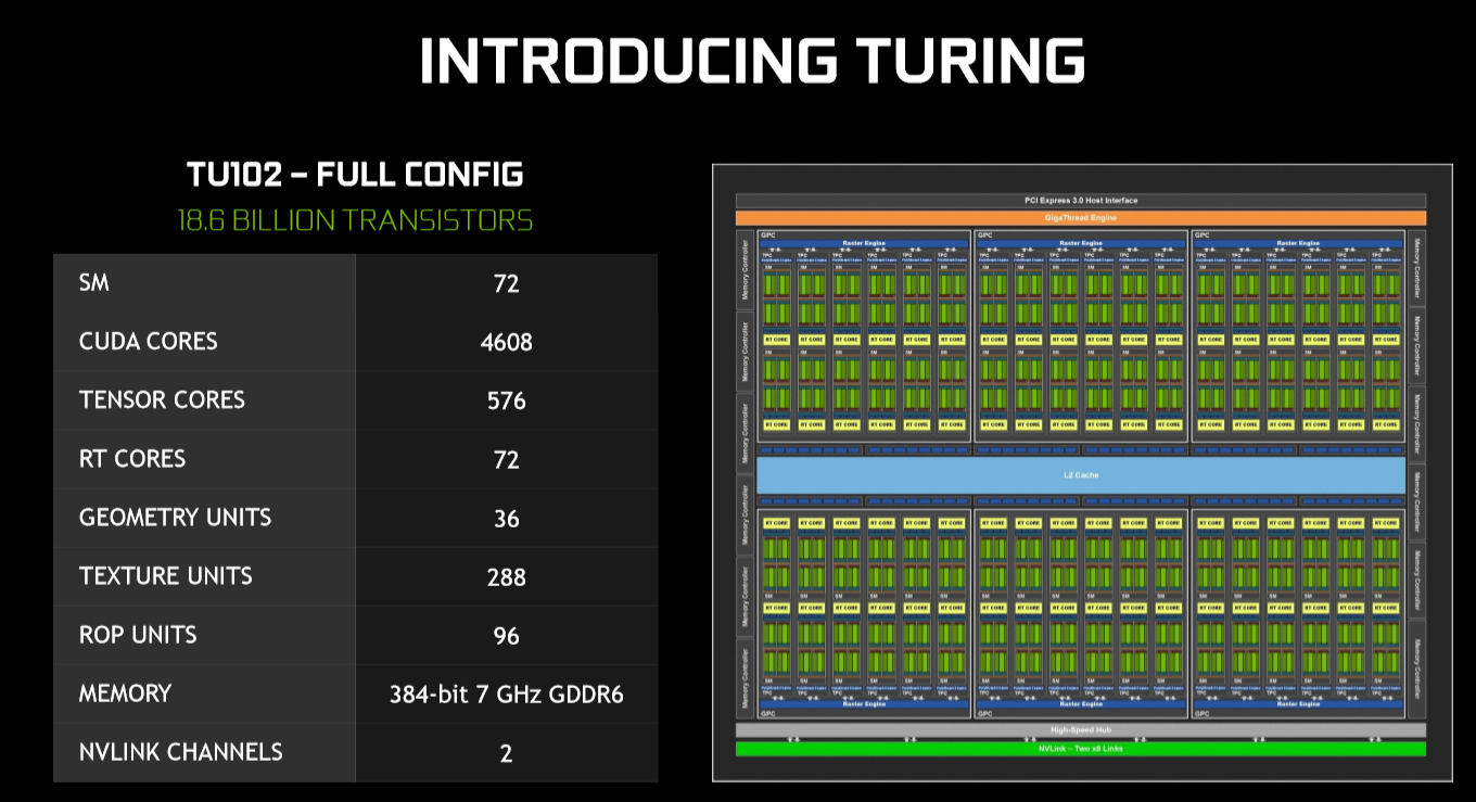
Here is a very high-level overview of the full-fat Turing TU102 block diagram. This is what's traditionally known as the 'big-die' part, and Nvidia usually releases it some time after the smaller, less complex mainstream dies. For it to come out first is interesting strategy that looks to squarely appeal to the well-heeled enthusiast before catering for the masses.
Though it may seem like a reasonable facsimile of the Pascal GP102 on first glance, they are quite different, and also continuing an Nvidia theme, the full-config TU102 won't be productised at launch time. What you will get is the RTX 2080 Ti that uses a slightly cut-down version of this monster GPU. If full-config TU102 does make a bow, it will be on a Titan-class card, we imagine. The numbers are massive no matter which way we cut it. 18.6bn transistors, three types of processing cores, and the fastest memory ever seen on a consumer card.
Massive really is an apt descriptor because the transistor count is 55 per cent larger than GP102, despite having only 20 per cent more floating-point shaders. It's huge, too, with a die-space area of 754mm² compared to GP102's 471mm². That silicon real estate is put into sharper relief when you consider Nvidia is using an optimised 12nm FinFET production instead of the larger 16nm.
How has this come to be? How can it be so big without, on paper, appearing to be that much faster when judged on CUDA cores alone? Nvidia has made a number of design choices that it reckons will pay off somewhat now but more so in the future. There are specific INT32 cores, those new Tensor cores, RT cores, more on-chip cache, and more register-file space, to name but the obvious die-space culprits. Get the feeling this is more of a workstation-type card reimagined than a pure gaming GPU? That's the choice Nvidia made by betting big on the types of technologies future games will employ.
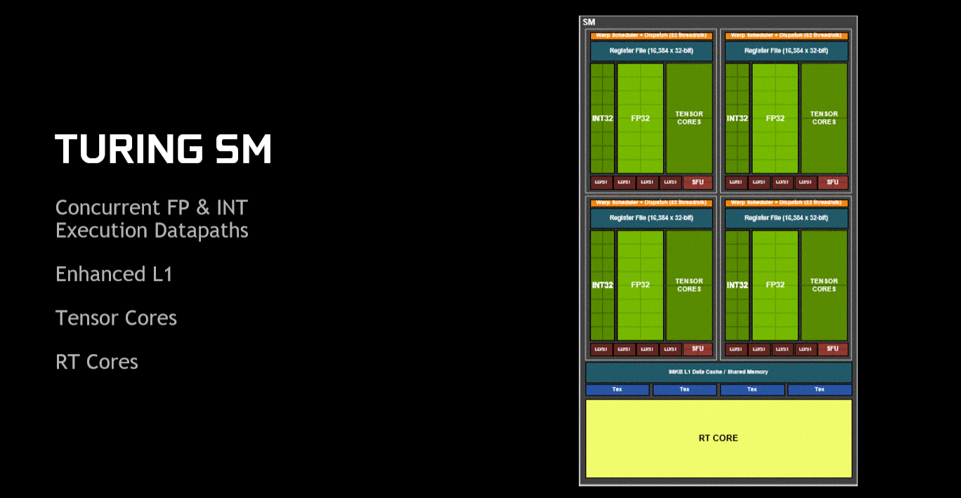
Right-o, let's dig deeper. You know how we mentioned that Turing takes liberally from the Volta playbook? That's in evidence when looking at one of Turing's SM units. The biggest change from Pascal is that Nvidia now puts in 64 FP32 and 64 INT32 (floating point and integers, respectively) into each SM, rather than have 128 FP32. Still, counting CUDA cores properly means only taking the FP32 into account, so each SM has half the CUDA cores as Pascal.
That number is turned on its head when you see that there are, potentially, 72 SMs in Turing, compared to 30 for Pascal in its finest Titan Xp (GP102) form. That means, in direct comparison, there are 4,608 FP32 vs. 3,840 FP32, plus an extra 4,608 INT32 for good measure on Turing. We'll explain why the latter has been introduced a bit further down the page. What you don't see is that each SM is home to a couple of FP64 units, mostly to ensure that any code that requires double-precision support runs correctly. The DP-to-SP speed is 1/32nd, so it's more of a feature tick-box than anything really useful.
An interesting by-product of going for more SMs with fewer FP units is what you can do with other bits of the design. You can change the ratio of texture units per shader unit but Nvidia has not chosen to do so; texturing capability isn't that important anymore. What it has done, however, is keep 256KB for register files per SM. Doing simple maths tells us there is more than 2.4x the total register-file space on TU102 compared to GP102, and the consensus is that increasing these, which constitute the fastest type of memory used for in-flight operations, helps enable quicker completion of threads. We guess Nvidia wanted to reduce instances of what is known as register pressure, where a lack of available registers forces the GPU to run to much slower local memory. This is purely a GPU design decision that increases the die size over the previous generation but the additional silicon cost is considered worth it from a performance maintenance point of view.


