The lasers!
Yes, this is the bit about the lasers! One of the problems we at HEXUS like to rant about from time to time is the lack of bandwidth between CPU, memory and other devices. We tend to point the finger at Intel more than AMD, but the problems exist for all processing platforms.
So, when we're talking about Tera-flops and terabytes, how is that data shifted around? Clever software and compilers help, but only so far. High bandwidth interconnects are required, which is where light comes in.
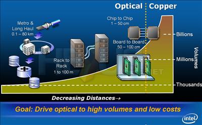
The bandwidth that can be carried by fiber optics is vastly greater than the data that can be sent electrically over copper. The only trouble with fiber is that it's mighty costly. Currently, optical interconnects tend to be used only when running relatively long distances, be it between networking components or between buildings and so on. Inside of components, copper still reigns supreme.
One of Intel's goals is to drive optical interconnects deeper into systems. From inside racks to in between circuit boards, then further still to the point where discrete chips are connected over fiber. There are numerous problems in getting fiber inside of computers, including the cost and size of light sources, and modulating/detecting the signals to provide a sufficient data rate.
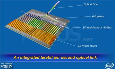
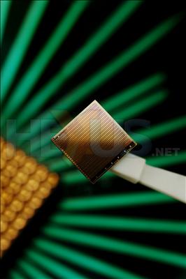
Intel's working in partnership with UCSB with the aim of producing chips with many hybrid silicon lasers that'll enable terabit speed optical data interconnects. So what are these hybrid silicon lasers?
Providing a light source for an interconnect is one of the big problems. With a laser set off the chip, there are alignment, power, attachment and cost issues. A directly attached laser is less expensive, but also has alignment issues along with a necessity for bonding with gold. A better solution, then? That'd be the hybrid silicon laser. An indium phosphide based material is bonded directly to the silicon chip; many can be bonded in a single process and no alignment of the light source is required. Ultimately, it should prove lower cost, too.
Intel and UCSB are using a plasma process to produce a 'glass-glue' that bonds the light source to the silicon wave guide. It's better than growing crystals and the bond is around 25 atoms thick.
With multiple hybrid lasers, each with wave guides setup to give different wavelengths, data can be multiplexed together and sent over a single fiber link. At the other end it can be demux'd and read. Combine an array of hybrid laser transmitters and a receiver unit onto a chip and bang, you've got a silicon chip with a fiber optic interconnect built right into it.
Networking
So once we've got these swanky new laser powered interconnects, how are we going to use them? One option is to have a mesh system in place. Much like the Internet, a mesh creates more than one way to get data from one place to another. If there are bottlenecks or failures within a mesh system, data can flow around the problem.
What about memory, though? Intel's been mentioning integrated memory controllers (haven't we heard of that idea before?). Taking it further though, is die-stacking. Take your memory and stack it up with multiple interconnects.
Oh, and one last thing for you to think about. With fiber on chips themselves, there's potentially a network interface right there. That's one hell of a high bandwidth, low latency network interface.


