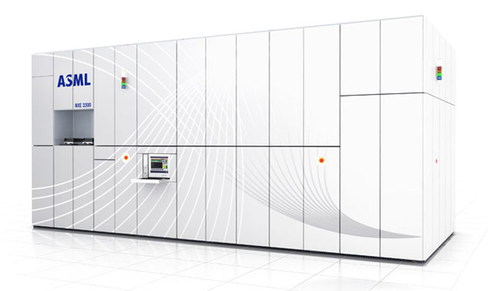
Extreme-ultraviolet (EUV) lithography offers some hope in the battle to keep Moore's Law relevant. The very short light wavelength that can be leveraged by EUV machines means that they have the capability to create higher resolution surface etchings than ever before, to help make components smaller than ever before. Now, according to MIT Technology Review, via Fudzilla, the first test machines capable of EUV lithography have started to ship, from chipmaking equipment firm ASML, to the likes of Samsung, Intel and others.

Back in 2012 HEXUS reported on Samsung making a considerable investment in Dutch company ASML which seems to be at the forefront in efforts to make EUV lithography practical for mass production. Samsung's cash backing followed even larger investments in ASML by chipmakers like TSMC and Intel.
Progress with EUV seems to have been slow. The problem was that it was difficult to make an EUV light source bright enough for practical industrial lithography processes. ASML has pushed forward with advances in plasma and laser physics and materials science to push past this hurdle. Over recent months it has managed to make the EUV light generator five times more efficient with the knock on effect of faster and more efficient lithographic process. But there's still room for improvement.
Of course ASML must now be feeling confident enough that its EUV machines are capable of impressing, or at least meeting its investors' expectations, as test machines have now shipped. Speeds quoted by the MIT Technology Review site suggest the test machines are capable of outputting something like 400 wafers per day. If the EUV light source could be doubled in intensity then up to 800 wafers could be output per machine per day. That is still said to compare unfavourably with status quo technology, capable of 3,000 wafers per day. However that 3,000 figure is expected to drop as more lithographic patterning steps and more expensive masks are required to make ever finer features on future chips without EUV.


