Back at Computex in June, AMD ended its keynote address with a very interesting segment where it introduced a Ryzen 9 5900X CPU prototype with added 3D V-Cache. We learnt that this prototype was the result of AMD's first practical implementation of 3D chip stacking technology. The firm targeted the CPU cache for this modification, as it was clear it would provide immediate benefits to multiple workloads.
Slides shared at Computex showed that the 3D V-Cache enhanced prototype delivered 15 per cent faster gaming on average thanks to the massive bandwidth boost that stacking a 64MB 7nm SRAM onto each CCD using TSVs provided. AMD CEO Dr Lisa Su said the first high-end Ryzen processors using 3D V-Cache would enter mass production in Q4 this year.
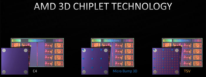
At Hot Chips 33, AMD has provided some more background about its use of 3D packaging technology in upcoming processors. ComputerBase has published a write-up and a bountiful selection of presentation slides from AMD's presentation. Above, you can see that the TSV connections used by AMD for its 3D V-Cache connection are much denser than previous/rival technologies offer.
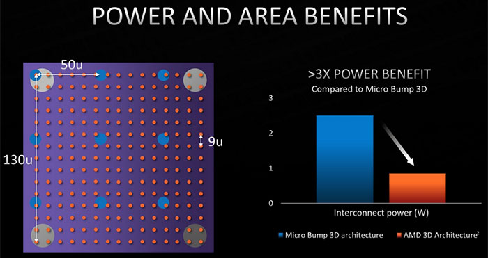
AMD focuses its comparisons on micro-bump 3D inter-chip connectivity which is far coarser (15x less dense), requires 3x greater interconnect power, and suffers from poorer capacitance and inductance characteristics.
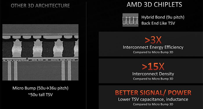
Above you can see AMD is boasting of a '9u pitch' – which is much denser than micro bumps, or even Intel's Foveros Omni technology with a 36u pitch. However, in 2023 Intel is going to start creating Foveros Direct chips with <10u pitch.
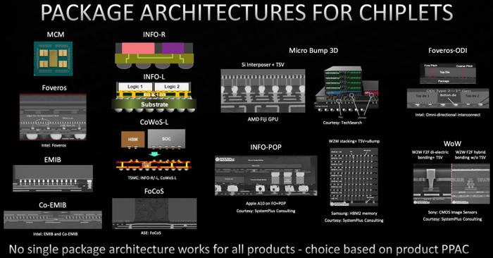
AMD is also working closely with partner TSMC on more advanced and complex 3D stacking technologies. It makes it clear, though, that while modular design is the way forward, not all types of chips benefit from the same 3D packaging strategies. As the slide above explains, an optimal choice must be based on PPAC (power, performance, area and cost).
AMD AM5 platform leak
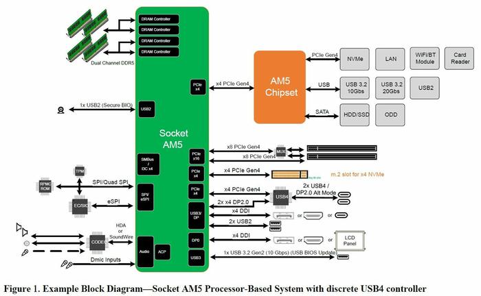
Documents that have leaked as a result of the recent Gigabyte hack attack have precipitated a few tech articles in recent days. A block diagram of the AM5 socket/chipset was put under the spotlight by TechPowerUp on Friday. It shows that of the platform will support dual-channel DDR5, but will be limited to PCIe 4.0.
Specifically, AM5 platforms will support 28 PCI-Express Gen 4 lanes. "16 of these are allocated toward PCI-Express discrete graphics, 4 toward a CPU-attached M.2 NVMe slot, another 4 lanes toward a discrete USB4 controller, and the remaining 4 lanes as chipset-bus," says TPU.
AMD moved to PCIe 4.0 over a year ahead of Intel with its Rocket Lake desktop processors, so it is interesting to see AMD cede PCIe 5.0 leadership to Intel. Intel has already confirmed that its Alder Lake-S motherboards will support DDR4 or DDR5, depending on the board you buy. The upcoming Intel desktop platform is also going to support up to 16 PCIe 5 lanes and a number of PCIe 4/3 lanes.
Another advance for AM5 that we can see in the block diagram is the provision of two 20Gbps USB 3.2 ports.


