The Raspberry Pi Pico was released on 21st January at a price of just US$4. The Pico is a microcontroller - a device-class often paired with a more powerful computer for analogue input and low-latency I/O, and sometimes a very-low power standby mode. One of the most interesting things about the Pico was that it became the first product to feature 'Raspberry Silicon', in the shape of the RP2040, and on Monday one of the engineers tasked with making this first in-house processor design wrote a blog on the whole process, entitled The journey to Raspberry Silicon.
The journey began in the summer of 2017. After deciding what fundamental components the RP2040 would require, design went ahead using industry standard tools like Verilog and VHDL. Testing and verification was done first in simulation, and as things become more advanced the design team started to use FPGAs. Even the fastest FPGA's the chip designers used only ran at 48MHz, while the final RP2040 production chip would run at 133MHz.
After various debug and refinement stages the RP2040 boot ROM was developed on FPGA, and code was run from an SD card equipped board – as hardware, firmware, and software were pulled together for the first time. After further refinements the Verilog chip design files were converted to logic cells – in this case – for manufacturing by TSMC using its standard cell library.
The first test chips were output by TSMC for engineers at the Raspberry Pi org to assess on bring-up boards. Using this modular board the RP2040 was put through its paces in simple operational tasks and some tasks similar to what it will end up being used for – all the time monitoring things like performance, temperature and power consumption.
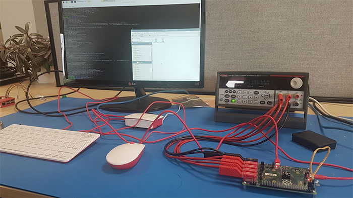
The USB boot mode working straight out of the box on a bring-up board
If all is well, and this appears to have been the case for the first slivers of Raspberry Silicon, the green light is given to TSMC to mass produce the chips. It probably won't surprise you that the RP2040 is a rather tiny 2mm2 chip, even though it is manufactured at 40nm by TSMC. The silicon is at the heart of a 7mm x 7mm QFN-56 package containing:
- Dual-core Arm Cortex-M0+ @ 133MHz
- 264KB (remember kilobytes?) of on-chip RAM
- Support for up to 16MB of off-chip Flash memory via dedicated QSPI bus
- DMA controller
- Interpolator and integer divider peripherals
- 30 GPIO pins, 4 of which can be used as analogue inputs
- 2 × UARTs, 2 × SPI controllers, and 2 × I2C controllers
- 16 × PWM channels
- 1 × USB 1.1 controller and PHY, with host and device support
- 8 × Raspberry Pi Programmable I/O (PIO) state machines
- USB mass-storage boot mode with UF2 support, for drag-and-drop programming
The Pico board adds 2MB of Flash memory, and a power supply chip supporting input voltages from 1.8-5.5V, a push button, and LED, as well as exposing 26 of the 30 GPIO pins on RP2040, including three of the four analogue inputs, to 0.1-inch pitch pads.
In the time between the signing off and the delivery of chips from TSMC and the assembly of the Pico microcontrollers the Raspberry Pi team worked for several months writing the SDK "and excellent documentation," available for product purchasers from day one.