In the wake of the recently published Q1 2019 results, TSMC's Vice Chairman & CEO C. C. Wei provided some interesting information about the firm's progress, in an earnings call. Just as we are seeing the first 7nm products reach PC enthusiasts, such as the recently released AMD Radeon VII, and AMD's 7nm fabricated Ryzen 3000 series of CPUs are on the verge of release, TSMC is ploughing on with its 6nm and 5nm plans. TSMC refers to its 7nm process as N7, and 6nm and 5nm processes as N6 and N5, respectively, and I shall be doing the same from now on in the article.

Wei told investors that there are currently many customer N7 chip tape outs in the fields of HPC, IoT and automotive. In the meantime N7+, which adopts EUV for a few critical layers, has already started volume production. N7+ yields are comparable to those from N7. Wei asserts that N7 and N7+ will contribute more than 25 per cent of TSMC wafer revenue this financial year.
Moving on to N6, Wei cited three main advantages. Firstly, it is 100 per cent design compatible with N7 for easy migration and shortened time to market. Secondly, N6 products can deliver 18 per cent greater logic density compared to N7. And thirdly, N6 will offer shortened cycle time and better defect density, according to Wei. He added that Risk production of N6 is scheduled to begin in first quarter year 2020 with volume production starting before the end of 2020.
"N5 technology development is well on track," said Wei. N5 entered risk production in Q1 2019, with some customer tape-outs starting this quarter and the volume production ramp expected in H1 2020. The TSMC VC and CEO highlighted that a sample ARM A72 core produced at N5 delivered an 80 per cent greater logic density with 18 per cent speed gain compared to N7. "With the best density, performance, power and the best transistor technology, we expect most of our customers who are using 7-nanometer today will adopt 5-nanometer," added Wei.

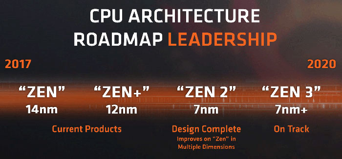
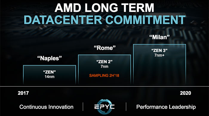
AMD Zen 3 based CPUs pencilled in to use N7+ in 2020
N5 will be a large and long-lasting node at TSMC concluded the executive. However, in a later question Wei admitted that customers would need some time to get up to speed for N5, while moving from N7 to N6 requires only "a very minimal effort".

AMD has already pencilled in using N7+ for Zen 3 CPUs and the post-Navi GPU architecture. From the above explanations from CC Wei we know that could easily transition to N6. However, the bigger benefits from N5 look set to occur in the next-next generation architectures designed by the likes of AMD.


