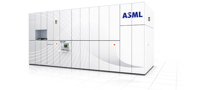
At the Semicon West tradeshow in San Francisco last week lithographic machinery vendor ASML announced that it had achieved an important and long-elusive milestone, reports the EE Times. ASML has successfully demonstrated a 250-watt EUV source which will accelerate wafer throughput up to about 125 wafers per hour (WPH). Industry watchers had seen the inability of ASML to reach this throughput figure as a major roadblock in EUV development.

There certainly has been progress shown by ASML. Source power is "a measurement of the amount of EUV photons delivered to the scanner to enable wafer exposure," explains the EE Times. Back in 2012 source power was limited to 25 watts so this news marks a 10 fold increase.
The achievement means that chipmakers such as Intel, Samsung, TSMC and Globalfoundries could cost effectively integrate EUV into their high-volume production lines. In Feb ASML demonstrated throughput of 104WPH but now with 125WPH being reached (that's 3,000 wafers per day) company engineers can finally congratulate themselves on a target met.

ASML's EUV machines cost over $100 million each and Intel is said to be buying the majority of the 21 of these EUV production tools on back-order since April. With the 125WPH target met, the EUV tools could provide a significant cost benefit with faster cycle times, fewer variables and fewer chances for random defects on wafers, according to ASML's director of strategic marketing, Michael Lercel.
EUV is seen as one hope in keeping Moore's Law relevant as it can create higher resolution surface etchings than ever before, to help make components smaller than ever before. The ASML TWINSCAN NXE:3400B will support EUV volume production at the 7 and 5nm nodes, for example.


