Fitting in with the tick-tock clock
Since 2007 Intel has adopted a tick-tock design philosophy to chip design, where a brand-new architecture is released in one year (tock) and then followed roughly a year later by a newer revision that improves upon the architecture by shrinking the process technology together with rudimentary design refinements (tick).
Going by Intel parlance, the 45nm-based Nehalem microarchitecture that debuted in November 2008 was considered a tock, while the Westmere iteration - shrink to 32nm, plus minor design improvements - brought to market in early 2010 was a tick.
Sandy Bridge will introduce the next tock in the paradigm, bringing a brand-new architecture to the table, which is based on the present 32nm production found in current Westmere chips.
Delving deeper
Intel's David Perlmutter explained that the Sandy Bridge microarchitecture will be the second Intel design to integrate the graphics component directly on the same die - as opposed to the same package, a la Westmere - as the CPU itself. On a high-level overview, bringing DX10.1-compatible graphics and the CPU truly together enables Intel to control more of the platform.
From a technical viewpoint, using the same die brings some synergistic benefits such as lower latencies - through what Intel term a scalable ringbus interconnect structure - cache sharing between GPU and CPU, and better control over how the Sandy Bridge chip uses its total power allocation (TDP) to maximise performance between code run on the CPU and GPU cores: better Turbo Boost, if you will.
The Sandy Bridge microarchitecture's integrated graphics are also functionally better than the current generation's. Intel inferred that the top-line parts will be twice as fast as the HD Graphics in Westmere chips. This informs us that the new IGP will genuinely rival the performance from discrete low-end cards, although, interestingly, Intel brushed away the need for DX11-class graphics for CPU IGPs.
A newer design means that Intel can drop some of the more legacy aspects of previous GPUs. Out goes LVDS as the display output of choice, to be replaced by DisplayPort, which is cheaper to implement and uses fewer wires.
Sandy Bridge to replace Lynnfield?
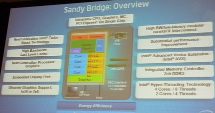
A look at a basic block diagram of Sandy Bridge shows that the microarchitecture is ostensibly designed to replace the mid-range LGA1156 parts available today. Sandy Bridge is to be presented with a different socket, LGA1155, and it'll use a dual-channel DDR3 memory controller, a DMI connection to the rest of the system, and external graphics support through 16 PCIe lanes, which is able to be bifurcated to two x8 for multi-GPU usage. In this aspect Sandy Bridge is eerily similar to incumbent Lynnfield, though users will be forced to shell out for new motherboards to take advantage of the chip.
Beefed-up CPU and dedicated video engine
Coming back to the CPU, which is mainly based on the Westmere core, the modular nature of the design and use of a ringbus cache support means that Intel can scale cores from two to eight without too much difficulty and bring different designs to market quickly. This indicates that Sandy Bridge should be introduced for laptops and desktop machines at roughly the same time, Q1 20100, with servers due to follow in late-2011.
The cores also deliver a greater number of instructions per clock cycle (IPC), mainly due to better cache implementation and the introduction of AVX (Advanced Vector Extensions), which include 12 new instructions and a doubling of the SIMD vector registers. These will help speed-up applications which rely on significant floating-point power.
What's more, Sandy Bridge includes a dedicated transcoding engine to make converting video formats a doddle - and perhaps introduced to combat the rise of GPGPU-based convertors from AMD and NVIDIA. It's not yet known if it's a fixed-function unit or whether it taps into the chip's IGP shaders to provide the processing grunt. More details as we get them.