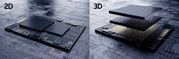
Samsung Electonics has announced that its silicon-proven 3D IC packaging technology, dubbed eXtended-Cube (X-Cube), is now available to customers. It claims to enable "industry-first 3D SRAM-logic working silicon at 7nm and beyond," and it leverages Samsung's through-silicon via (TSV) technology. Most importantly, X-Cube is claimed to deliver "significant leaps in speed and power efficiency."
"Samsung's new 3D integration technology ensures reliable TSV interconnections even at the cutting-edge EUV process nodes," said Moonsoo Kang, senior vice president of Foundry Market Strategy at Samsung Electronics. "We are committed to bringing more 3D IC innovation that can push the boundaries of semiconductors."

In its own X-Cube test chips, Samsung engineers built a logic die with SRAM stacked on top. The TSV tech, as previously championed in its memory chips, was used here to fuse logic and memory into a smaller footprint. Package size isn't the only benefit, the resulting 3D integrated component features significantly shorter signal paths between the dies for maximized data transfer speed, reduced latency, and energy efficiency.
Samsung says X-Cube is now available for partners on advanced nodes such as 7nm and 5nm. Of course, it hopes to attract many fables customers to use the tech and benefit from it.
3D packaging has helped the RAM and flash memory market move forward significantly. Intel has championed similar tech since 2018 for use in SoCs. Its 3d integration tech is called Foveros, and it is key to the new Lakefield chips, which also implement a hybrid architecture.
Samsung promises to reveal more about X-Cube at Hot Chips 2020, which runs from 16-18th August.


