Researchers at the University of California Santa Barbara and Rice University have designed a transistor that can switch at voltages as low as 0.1V. This Tunnel field effect transistor (TFET) could bring great energy efficiency to electronics as it reduces power dissipation by 90 per cent compared to state-of-the-art silicon MOSFETs, reports the EE Times.
The problem the researchers are seeking to address is described as follows: "MOSFETs have been the building blocks of everyday electronic products since the 1970s. However, to sustain the ever-growing need for increased transistor densities, miniaturization of MOSFETs has given rise to a power dissipation challenge due to the fundamental limitations of their turn-on characteristics."
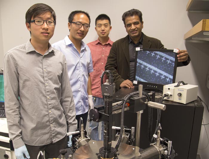
Kaustav Banerjee, Professor of Electrical and Computer Engineering at UC Santa Barbara, explained why TFETs have a power advantage over MOSFETs "The steepness of a transistor's turn-on is characterized by a parameter known as the subthreshold swing, which cannot be lowered below a certain level in MOSFETs". In the case of MOSFETs at room temperature that steepness is 60mV/decade but it is approximately 30mV/decade in the tunnel field effect transistor (TFET) detailed in the recent research paper.
Prof Bannerjee and colleagues
The TFET used by UCSB and Rice University is built with a molybdenum disulfide single atomic layer (1.3nm) as the current carrying channel, placed over a germanium source electrode. This 'flat transistor' offers superior properties than TFETs built with silicon or III-V compound semiconductors, says the EE Times, as they are less likely to suffer from current leakage.
Prof. Banerjee described the UCSB TFET engineering feat as "the thinnest-channel subthermionic transistor ever made". The use of 2D materials such as molybdenum disulfide provides a boost to the technology, providing a major step forward in the search for a low voltage logic transistor.