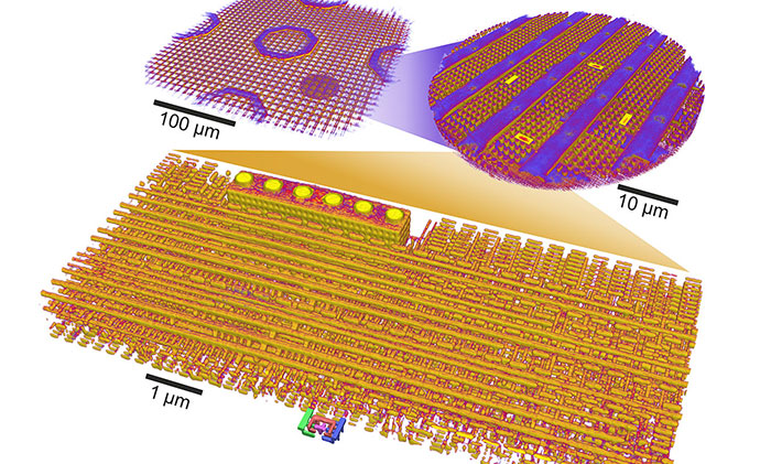
Researchers from the University of Southern California and the Paul Scherrer Institute (PSI) in Switzerland have developed a useful new semiconductor imaging technique. The new ptychographic X-ray laminography technique means that modern 3D designed computer chips can be reverse engineered or verified - non-destructively.

Previously 3D chips would need to be progressively ground down, cuts made, and then various imaging techniques applied in order to reverse engineer or verify its design. Now the US/Swiss research team's ptychographic X-ray laminography technique can image a chip without cutting into it. The chip will, however, need its surface to be polished down to 20 micro metres thickness.
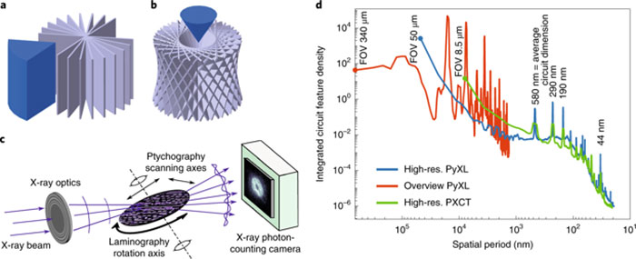
After the chip surface is minimised an 3rd gen synchrotron X-ray beam is focussed at a 61 degree tilt and the chip rotates on a stage to reveal its inner construction. A lower resolution scan can complete in 30 hours but areas of interest can be scanned in an additional 60 hours - in enough detail to "identify the parts of an individual inverter circuit in a chip made using 16nm".

Potential 10,000x scanning speed uplift, 2nm part scanning
While it might seem slow right now, there are newer 4th gen X-ray machines in the pipeline which will be able to reduce the initial low res scan time to under an hour, for example. The researchers assert that over the next five or six years scan imaging time will be improved by 1,000 - 10,000 x speeds. Furthermore, the system will be able to comfortably handle 7nm parts, they assert, going down to 2nm in the future.
Design fingerprints
The new chip scanning system is seeing a lot of interest from US national security bodies. Of course such organisations will be not particularly interested in reverse engineering chips but rather be looking at deviations from design to manufacturing. They will be able to check for kill switches, hardware trojans and similar issues which may have been introduced to chips for nefarious purposes. Moreover, Anthony F. J. Levi, professor of electrical and computer engineering at USC explained that "You can identify the foundry, aspects of the design, who did the design. It's like a fingerprint".
Sources: Electronics Weekly and IEEE Spectrum.


