A team of researchers at the University of Delaware (UD) have successfully tested a lens built at microchip scale on top of a silicon wafer, using specialised thin metasurface materials. This could be a key step in shrinking all the elements of traditional photonics down to microscale, enabling optical microcomputing, next-generation compact LiDAR units, on-chip spectrometers, and quantum information processing.
To solve the problem of downsizing the optics UD researchers including Tingyi Gu, an assistant professor of electrical and computer engineering, have built a lens from a metasurface material on top of a silicon wafer. Issues of signal loss with previous 'plasmonic' metasurface materials were side-stepped by creating a new kind of metasurface made from etched dielectric materials atop of silicon wafers. This material creates a 'lens' that introduces a signal loss of less than one dB - reducing potential for unwanted heat and noise from the design. Now, thanks to the new dielectric metasurface lens, "we can make a device much smaller and more compact," asserted Gu.

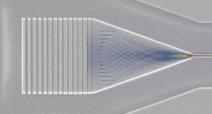
If you look at the diagram above you can see an image of an on-chip micro-sized lens, created at UD by the researchers (with simulated light response superimposed). It is made from various gratings etched upon the silicon in the special materials, and it exhibited several of the key properties of a traditional glass lens in the tests - "including converging beams with a measurable focal length (8 micrometers) and object and image distance (44 and 10.1 µm)," notes IEEE Spectrum.
Of course the grand plan is to put these micro-scale lenses into microchips. The speed-of-light devices are "going to be fast," said Gu. However, the team now has to start working on integrating these lenses into complex traditional electronic circuitry.


