facebook rss twitter

AMD Arctic Islands GPUs may employ 14nm FinFET tech

by Mark Tyson on 23 April 2015, 11:03

Tags: AMD (NYSE:AMD), TSMC, GLOBALFOUNDRIES

Quick Link: HEXUS.net/qacqwa

Add to My Vault: x

While we are still patiently waiting for any official announcement of the AMD Radeon R300 series there is much chitter-chatter on the web about AMD's plans going far beyond those GPUs. Various sources suggest that in 2016 AMD will being to unleash its 'Arctic Islands' GPUs which will be built using the 14 nm FinFET process and feature high performance, low power, higher density HBM2 memory.

Chinese language site EXP Review says that the first of AMD's Arctic Islands series will be the 'Greenland' GPU. Its report suggests that AMD, like Nvidia, will go straight from 28nm to 14nm GPU fabrication as 20nm "is too costly and not suitable for such a large core GPU". Fabrication at 20nm is said to be much more suitable for mobile/tablet SoCs and current capacity is almost all dedicated to Apple SoC manufacture.

Very little is known about the Greenland GPU other than that purported piece of information about its 14nm fabrication. Speculation is still rife upon what foundry would make the 14nm FinFET AMD GPUs; Global Foundries, TSMC, Samsung and Intel are all name checked in a TechPowerUp article about the future Arctic Islands GPU range.

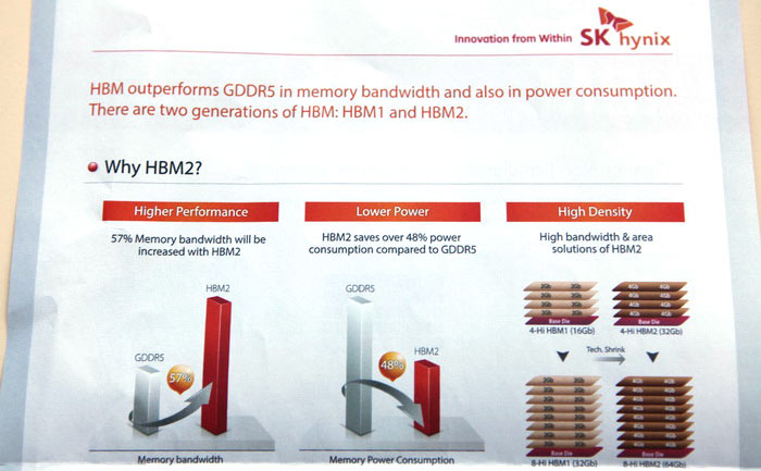
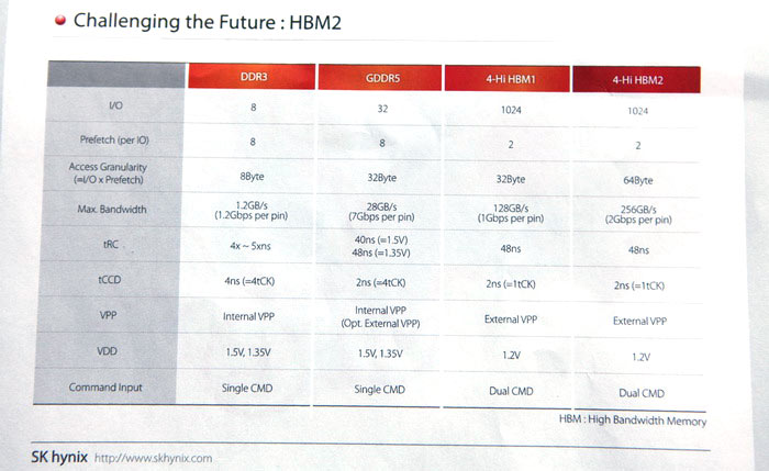
It is thought, or perhaps rather it is hoped, that the geographic location of the Arctic Islands hints at the cool, efficient nature of the range of GPUs which AMD will introduce in 2016. Greenland is purported to be a large GPU (it is a very large island). One thing we do know, is that if graphics card designs based upon these GPUs move to implement HBM2 memory (from the expected HBM1 on the high-end R300 series), that brings with it power consumption savings. Official SK Hynix documentation claims that HMB2 offers significantly better performance and power consumption than GDDR5 while providing a doubling in density compared to HBM1.


HEXUS Forums :: 10 Comments

Login with Forum Account

Don't have an account? Register today!
This sounds to me like: TSMC have messed up a whole bunch of nodes so everyone who's had to stay with 28nm is jumping to 14nm where they can buy from Samsung if they need to.
Not sure they messed up the nodes as making 20nm isn't a technical problem, it's more a costs problem.
Advanced Substrate News has a nice article on the costs involved.
Corky34
Not sure they messed up the nodes as making 20nm isn't a technical problem, it's more a costs problem.
Advanced Substrate News has a nice article on the costs involved.

But according to that article, you wouldn't go to 14nm FinFET either, as that's EVEN more expensive.

It seems some people are not at all happy with the 20nm products (eg qualcomm) despite them having been costed.
I'm not going to pretend to know the pro's and con's of FinFET vs FD-SOI when it comes to GPU design so I hope this article on PCPer from 2013 may help answer why there possibly going for FinFET.
kalniel
This sounds to me like: TSMC have messed up a whole bunch of nodes so everyone who's had to stay with 28nm is jumping to 14nm where they can buy from Samsung if they need to.

Believe you're spot on Kalniel, as 20nm has been a serious issue for GPU manufactures as TSMC have been unable to supply the demand (both in yield and time) it seems people are just skipping 20nm all together which is a good call in my opinion as it allows the next GPU generation to provide far greater efficiency while being similar in cost to 20nm (in terms of actually getting up and running with suitable yields).

In particular of AMD I believe this jump is valid as the 14nm FinFET is a collaboration between Samsung and GlobalFoundries so I presume AMD would have been able to get some preferential treatment from GF for a change, also the track record between GF and Samsung is much stronger than TSMC of late.

GPUs next year could be very interesting!