facebook rss twitter

AMD presentation reveals more details on Radeon HD 6900 architecture

by Pete Mason on 23 November 2010, 12:21

Tags: AMD (NYSE:AMD)

Quick Link: HEXUS.net/qa276

Add to My Vault: x

One of the take-home messages from our review of AMD's Radeon HD 6800-series graphics-cards was that the fundamental architecture really wasn't that different to the HD 5870 that preceded it.

It doesn't look like this will be the case with the upcoming HD 6900-series GPUs, though. According to slides from an AMD presentation - which just came out of NDA, in spite of the fact that the cards had been delayed - the company's engineers have made quite a few changes since we first saw the Evergreen architecture.

The biggest is that the GPU will be split into two identical graphics engines. If you compare the block diagrams to those for the HD 6870, you'll see that the shader engines now feed into two separate graphics engines which then recombine into a shared 256-bit memory controller.

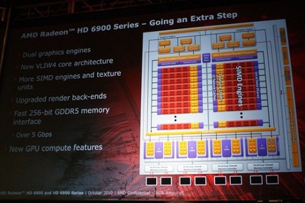
Both engines will also be tied to the same command processor and there will apparently be aggressive load balancing between the two. In essence, this means that the chip will function a bit like an advanced dual-GPU graphics card made of two cut back HD 6800-series chips.

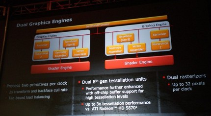
There are also optimisations to the tessellation engine, which AMD claims will let the HD 6970 outperform the HD 5870 by 200 per cent on average and by as much as 300 per cent in some scenarios.

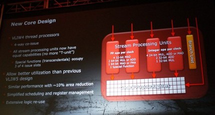
The streaming processor cores will see a major redesign as well. Whereas older GPUs from the company used a VLIW5 design with one 'smart' and four 'simple' units, the new cores will use a VLIW4 design where each unit is smart and capable of both floating-point and integer operations. This should allow for simpler resource management and similar performance in a space that's about ten per cent smaller.

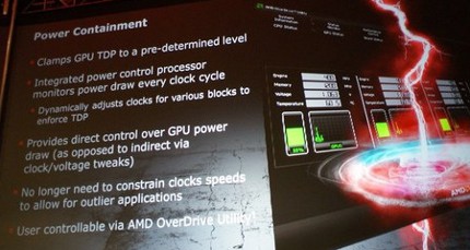
Rounding out the major updates will be new power circuitry that offers overclockers greater control over the board's power-usage. Now, instead of tuning a card by adjusting clock speeds and voltages the maximum TDP can be set and the on-board power circuitry will automatically and dynamically adjust the performance profile to fit within that thermal-envelope. Exactly how this will work remains a mystery, and it still isn't clear how much control overclockers will actually have.

Whereas the 'Barts' chips seemed like an efficiency tweak, the Cayman GPUs seem to be a legitimate overhaul to the Evergreen architecture and a worthy upgrade to the older cards. Unfortunately though, the clock speeds and shader counts weren't set at the time of this presentation, meaning that we still won't know for sure how AMD's latest and greatest will actually perform.


HEXUS Forums :: 4 Comments

Login with Forum Account

Don't have an account? Register today!
*sigh* confused now. Are we really going to have 3 different architectures in one series? We know the 68x0 is a tweaked 5800 architecture, so assuming the 69x0s are this new architecture with 4 ‘smart’ shaders per block (and a 16:1 shading:texturing ratio) and the 67x0 are going to be rebadged 57x0s, it would appear we are. Come on ATI, I know you've merged with AMD but there's no need to go that far to the “green” side… ;)
Deleted
*sigh* confused now. Are we really going to have 3 different architectures in one series? We know the 68x0 is a tweaked 5800 architecture, so assuming the 69x0s are this new architecture with 4 ‘smart’ shaders per block (and a 16:1 shading:texturing ratio) and the 67x0 are going to be rebadged 57x0s, it would appear we are. Come on ATI, I know you've merged with AMD but there's no need to go that far to the “green” side… ;)

I'd rather have different architectures under the same series than have different series for the same architecture ;)

But in this case they could probably argue that the core architecture isn't that different, it's just wrapped slightly differently.
The only people saying the 5770 will be rebadged, well, started on Fud I believe.

Think of it this way, take Barts core, which offers more performance per mm2, or take Cayman which offers more performance per mm2.

Now with two updated more efficient architectures meaning they can get the same performance out of a smaller core, as the wafers cost the same no matter what you make, the smaller the core the cheaper it is and the more you can make.

So the options presented, are continuing to make a 177mm2(iirc, somewhere around 170mm2 anyway) 5770's and call then 6770's, sell them for a reduced cost as their performance vs top of the line is reduced, less profit.

Use the barts architecture, with less shaders, get the same performance for around 35% die size space saving as seen on Barts, sell a card, thats 35% smaller for the same cost, and make 35% more profit?

Or use a cut down caymans, we aren't sure how much extra performance per mm2 it offers, and probably get more than 35% reduction in size for the same performance, and therefore make 40% more profit.

But Fud/Nvidia biased sites would have you believe AMD will choose to continue making a larger less profitable chip than necessary just for the hell of it? Sounds retarded, yup.


As far as I know the only reason someone decided it was to be rebraded was some slides show 6970/50, 6870/50, and an arrow that shows the 5770 being sold throughout Q4. It doesn't have 6770 listed anywhere ahead of that arrow, all the slide means is the 5770 is the midrange card through Q4 this year, meaning a replacement is due in Q1, AMD have not once said this will be a rebrand and I can't think of a logical reason for them to want to do so.

I'd say of the article, its a little off to say the 6970 is like 2 cut down 6870's, they share very little in common architecturally seeing as the large portion of the core is shaders, and the shaders are completely different.

http://www.hexus.net/content/item.php?item=20289&page=3

The only thing thats different in reality, is the graphics engine up the top, the shader blocks were always in two separate groups, the global data share was always there, basically, its easier to load balance 800 shaders worth of throughput in one engine and have two engines, than load balance 1600 shaders in one engine. As shader number increases this was almost always certain to happen.

When you compare the 6870 and the 6970, its not even remotely like theres two 6870's in there.

http://www.hexus.net/content/item.php?item=27053&page=2

Infact, there's your 6870, theres even less change between the 6870, the two shader blocks, the 2 separate thread dispatchers, the only fundamental(from terms of how data moves through the gpu) difference is the graphics engine has been split in two, and again with the 6870 having less shaders than a 5870, theres no real need to have two engines, with the 6970 and an increasing number of shaders, its pretty much expected. Considering it even has the same number of rops and general bits and bobs its even odder to call it “2 6870's”.

Then when you actually look at each individual piece of logic, there will be many differences, shader's have changed drastically, rops/tmu's/thread dispatcher are likely all slightly different. The seeming off chip buffering we heard of being the two extra rows of shaders below the main blocks.
Deleted
… As far as I know the only reason someone decided it was to be rebraded was some slides show 6970/50, 6870/50, and an arrow that shows the 5770 being sold throughout Q4. …

Well, there's always the rapidly pulled Catalyst PC Vendor ID List which listed the lower end 6000s as Evergreen. Sure, it could just be a slip of the copy & paste, but coming from AMDs own website it's rather suggestive.

Add to that the possibility that the profit margins they're already seeing on the lower end 5000s are sufficiently high that they can easily absorb a minor price snip, that they're also already performance competitive with their nearest nvidia rival (the GTS450), and they already sit at a price point that no other AMD card encroaches on, and it's possible that the cost of taping out and testing new silicon for the lower range isn't worth the potential increase in profit that a smaller die might bring. Why spend money creating a new design when your existing one fits the market requirements perfectly?