An AMD patent addressing active bridge chiplet design has been spotted by redditor marakeshmode. This new patent, published on 1st April, follows up similar works and a patent for a passive bridge between GPU chiplets filed in January. This body of work is evidence of AMD working to apply its multi-chip-module CPU chiplet strategy to GPUs. One important aspect of the new design to note is that the GPU chiplets with the active bridge would appear to developers as a single, monolithic GPU, so there would be no CrossFire style multi-GPU shenanigans required by game and app makers.
118 = active bridge containing L3 cache memory
Abstract:
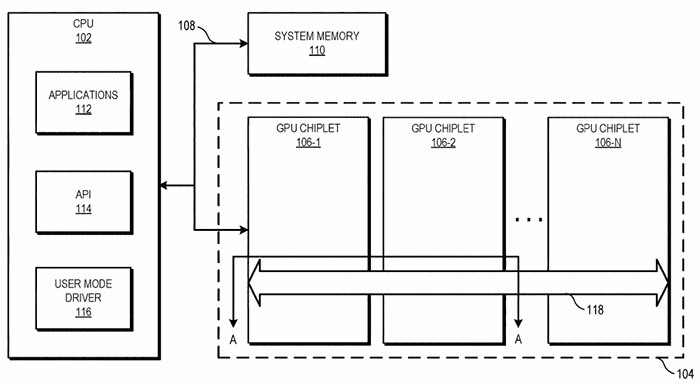
A chiplet system includes a central processing unit (CPU) communicably coupled to a first GPU chiplet of a GPU chiplet array. The GPU chiplet array includes the first GPU chiplet communicably coupled to the CPU via a bus and a second GPU chiplet communicably coupled to the first GPU chiplet via an active bridge chiplet. The active bridge chiplet is an active silicon die that bridges GPU chiplets and allows partitioning of systems-on-a-chip (SoC) functionality into smaller functional chiplet groupings.
Above is the official abstract for the new patent which is like an executive summary that encapsulates the idea being patented. Part of the driving force behind AMD's patents in this area is that "conventional monolithic die designs are becoming increasingly expensive to manufacture". The scientists admit that CPUs are naturally more suited to multi-chiplet designs, while the parallel compute workloads of GPUs tend to be more efficient when this quality is maximised. Additionally, applications tend to be written with the assumption that a system has just multiple CPU cores but one GPU.
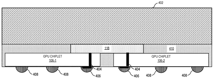
AMD's answer, indicated by this patent, is that chiplet GPUs will share an L3 cache and an embedded bridge to facilitate fast communication between the chiplets. The system CPU will be coupled with the first of the GPU chiplets but the L3 cache will remain coherent between all GPU chiplets present and maintain the 'massively parallel environment' of a large monolithic GPU. Chiplet GPU L3 cache is actually present on the bridge in this design and seems to be similar to the Infinity Cache on RDNA 2 architecture GPUs.
The above raises lots of questions about whether the chiplet GPU will have some drawbacks in practice. It may be that AMD will initially use its GPU chiplet patents in designs for accelerators for servers and data centres. That seems to be the MO of rivals working on MCM GPUs like Intel (Xe-HPC) and Nvidia (with the rumoured MCM architecture dubbed Hopper).