facebook rss twitter

AMD publishes GPU chiplet design patent

by Mark Tyson on 4 January 2021, 13:11

Tags: AMD (NYSE:AMD)

Quick Link: HEXUS.net/qaepyu

Add to My Vault: x

AMD's biggest GPU making rivals, namely Nvidia and Intel, are known to be working on chiplet-based GPU designs. Intel in particular has been very up front with raising awareness of what it calls Multi-Tile GPUs, for example check out this Xe family photo from June last year. AMD has effectively popularised chiplet CPU designs with its Zen series and one might wonder why the same approach to GPUs hasn't been taken by the firm as yet. Some answers may be found in the recently unearthed patent 'GPU Chiplets using High Bandwidth Crosslink' and the patent number 'US 2020/0409859 A1' (PDF link).

Primary chiplet

The patent documentation indicates that AMD's exploration of GPU chiplet designs has been slowed by it foreseeing two major hurdles to success – complexity and expense. Because of these concerns it is has kept its GPU designs monolithic so far, though as GPUs get bigger this is creating its own set of drawbacks. Now AMD's researchers and engineers are starting to see a path through the multi-chip GPU brambles, hence this new patent.

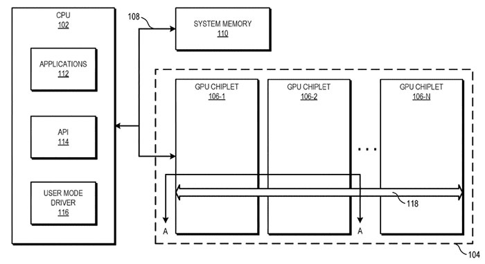
Multiple chiplets with HBX shown as connecting component 118 above

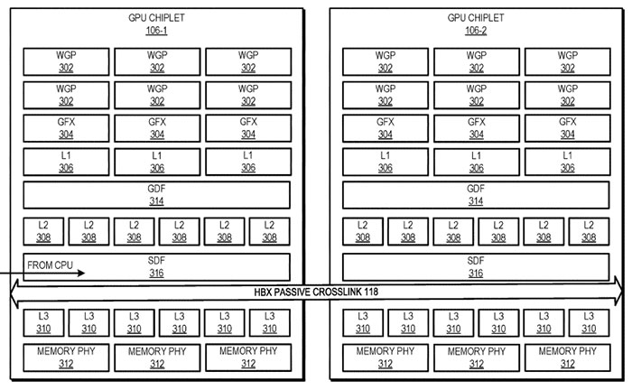
In the patent there is described a 'primary chiplet' which works alongside a driver layer to make the CPU believe it is still communicating with a monolithic GPU – this subterfuge should smooth any architectural transition process. The primary chiplet does some other tasks too – like intelligently distributing the computing load.

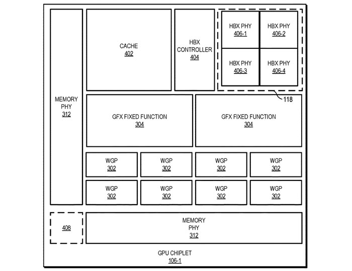
HBX position in more detail

An important part of the patent appears to be a passive interface called a High Bandwidth Crosslink (HBX). According to the patent this connects the L3 caches of all the chiplets so that they can access the cache data and VRAM accessible by all the other chiplets. Moreover, the diagrams indicate that a chiplet contains both L2 and L3 caches, similar to RDNA 2. Whether this means that the chiplet design is destined to a mainstream/gaming GPU remains to be seen. The patent shows dual chiplets connected along a line, as well as greater multiples in a star shape.


HEXUS Forums :: 10 Comments

Login with Forum Account

Don't have an account? Register today!
Makes sense to me, it clearly works on the cpu front and ‘gpu’s' are turning into more than just graphics cards these days so it only seems logical to me to expand the principle to the gpu front…especially on the ‘professional’ end of the ‘gpu’ spectrum.
Aww man, I got really excited for a second about AMD and GPU news… I’m very (im)patiently awaiting news on the 6700 and 6700 XT lol
My first thought was that it would be interesting if this brought about a resurgence in Crossfire/SLI style setups. With the primary chiplet managing resources it might be possible to combine CPU, discrete, dedicated RT cards & external GPU hardware in a good way. Either way it seems like AMD is heading towards offering a system that lets you build a single system with x86, x64, ARM, shader, RT & FPGA cores and plenty of bandwidth & fast interconnects between them all.
maxopus
My first thought was that it would be interesting if this brought about a resurgence in Crossfire/SLI style setups. With the primary chiplet managing resources it might be possible to combine CPU, discrete, dedicated RT cards & external GPU hardware in a good way. Either way it seems like AMD is heading towards offering a system that lets you build a single system with x86, x64, ARM, shader, RT & FPGA cores and plenty of bandwidth & fast interconnects between them all.
Crossfire was seen as 2 separate gpu's, this in the end was too complex to code for (well basically mantle and following low level api's killed it as it moved too much of the complexity from the gpu makers drivers to the application or game, and most game dev were not gonna put that sort of effort in to make it work).

Here the whole point is it is seen as 1 gpu. The problem there is the game dev is not coding it like they have a bunch of little linked but independent gpu's, they just expect it to work as 1 gpu. To do that every core has to work with every other core (sharing memory), and that means it will need to get data stored in one chiplets cache onto another one. No matter what impressive name they call the crosslink we end up with a massive bottleneck vs having everything in one chip.

The best way to fix this is actually know we have a chiplet setup, which you'd do by having a high level graphics api and smart drivers that sorted everything out so it could use the chiplets efficiently. Only AMD stuffed all that when they pushed everyone onto low level API's. Hence while we hear a lot about chiplets not convinced that it'll come to anything for gamers - gpu compute is obviously different.
LSG501
Makes sense to me, it clearly works on the cpu front and ‘gpu’s' are turning into more than just graphics cards these days so it only seems logical to me to expand the principle to the gpu front…especially on the ‘professional’ end of the ‘gpu’ spectrum.
The problem with doing it on GPUs is the latency, if they can work around that then it's a good path to go down, if however it adds to many nanoseconds to the pipeline it could end up being awful for things like gaming or VR.

For the ‘professional’ end of the spectrum i guess it would depend, i wouldn't fancy my self-drive car taking an extra 20-30 ns on every decision it's making, if it was making 1k decisions per second and we add 20-30ns to each of those decisions they soon add up.