Intel has used its platform this week at SEMICON West in San Francisco, to unveil its latest advance chip packaging technologies. In a blog post about the SEMICON reveal and presentation, Intel starts by explaining the importance of chip packaging technology, which it says has "always played a critical – if under-recognized" role in the electronics. It then asserts that chip packaging will play an even more important role in the future, before revealing three new technologies that "will open a new dimension in product architecture".

Babak Sabi, Intel CVP of Assembly and Test Technology Development, told SEMICON West attendees that "Our vision is to develop leadership technology to connect chips and chiplets in a package to match the functionality of a monolithic system-on-chip." Sabi added that "A heterogeneous approach gives our chip architects unprecedented flexibility to mix and match IP blocks and process technologies with various memory and I/O elements in new device form factors," and that Intel's company structure (chip design to foundry) gives it "an unmatched ability to co-optimize architecture, process and packaging". Furthermore, Intel sees packaging as a new catalyst for product innovation.

Co-EMIB
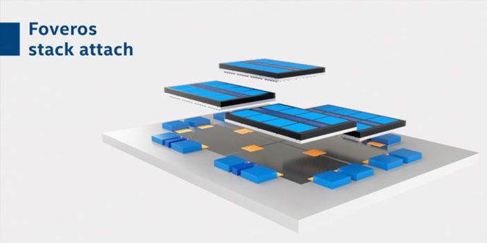
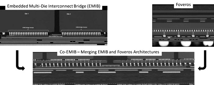
This technology melds Intel's EMIB and Foveros tech to deliver high bandwidth with low power consumption. It says its Co-EMIB tech delivers I/O density on par with or better than competitive approaches and "enables the linkage of even more computing performance and capability together". Using Co-EMIB chip designers can connect two or more Foveros elements alongside memory and other chip tiles with very high bandwidth.
ODI
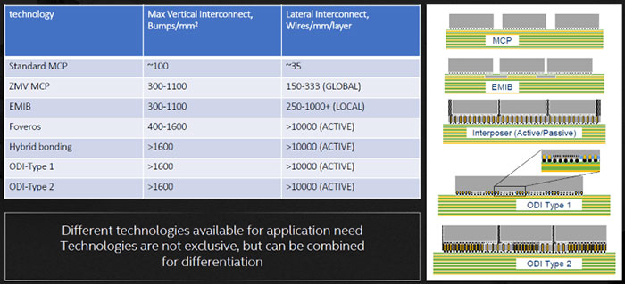
ODI is short for Omni-Directional Interconnect. As the full name implies, ODI adds a further dimension to chip packaging. It builds on EMIB horizontal communication with through-silicon vias (TSVs) in the base die below, similar to Foveros.

Intel says that ODI leverages much larger than traditional TSVs to allow power delivery to the top die directly from the package substrate with low resistance, higher bandwidth and lower latency. Moreover, ODI's approach means that the number of TSVs in the base die can be reduced and that provides more room for active transistors, making better use of the area.
MDIO
MDIO is Intel's newest die-to-die interface, building on the Advanced Interface Bus (AIB) PHY level interconnect. Thanks to MDIO Intel can enables a modular approach to system design with a library of chiplet intellectual property blocks. Importantly MDIO provides improved power efficiency with "more than double the pin speed and bandwidth density offered by AIB".
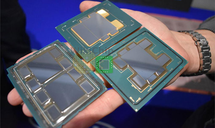
Intel says the combining of the above trio of tools provides a powerful toolbox for chip architects. WikiChip's David Schor was at SEMICON West and shared a 2020 Intel tech teaser as per the image below. Schor later added that the image shows "near reticle size 10nm compute dies with very aggressive bump pitch & aggressive wire spacing utilizing EMIB w/ other near-reticle size compute dies, HBM, & other dies".

Don't mention the glue


