facebook rss twitter

Intel shares Goldmont Plus microarchitecture information

by Mark Tyson on 29 December 2017, 11:01

Tags: Intel (NASDAQ:INTC)

Quick Link: HEXUS.net/qadpa2

Add to My Vault: x

Earlier in December Intel introduced its all new Intel Pentium Silver and Intel Celeron processors. Six new processors were released to systems and device makers and we should see the first fruits bearing these SoCs soon, in Q1 2018. Intel's new Goldmont Plus microarchitecture was the basis for its recent Gemini Lake platform launch and, as a reminder, it replaced the Goldmont microarchitecture that powered Apollo Lake chips.

At the time of the Pentium Silver launch we got a broad brush strokes rundown of the new processor ranges' attractions. They sported perkier performance, better modern graphical capabilities, improved networking, and were said to be very energy efficient. However, we didn't learn much in the way of technicalities on what was different from Apollo Lake.

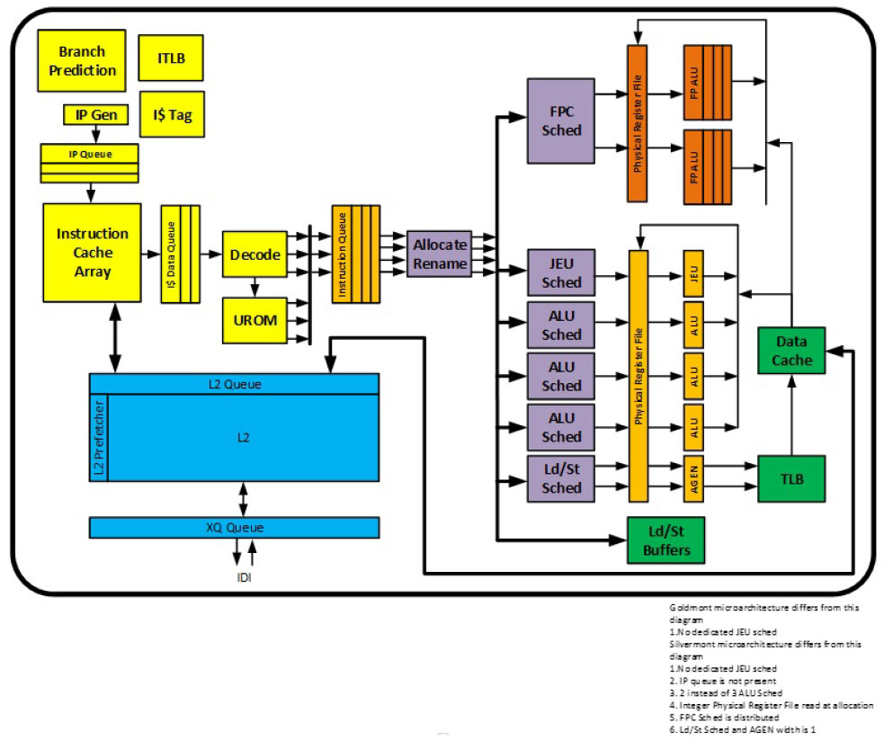
Now Intel has shared some further architectural information regarding the Goldmont Plus microarchitecture. In a PDF reference manual aimed at developers (link, go to chapter 16) Intel shares a list of architectural enhancements over the original Goldmont microarchitecture and a CPU diagram. Below is the full list of enhancements present taken directly from the PDF:

  • Widen previous generation Atom processor back-end pipeline to 4-wide allocation to 4-wide retire, while maintaining 3-wide fetch and decode pipeline.
  • Enhanced branch prediction unit.
  • 64KB shared second level pre-decode cache (16KB in Goldmont microarchitecture).
  • Larger reservation station and ROB entries to support large out-of-order window.
  • Wider integer execution unit. New dedicated JEU port with support for faster branch redirection.
  • Radix-1024 floating point divider for fast scalar/packed single, double and extended precision floating point divides.
  • Improved AES-NI instruction latency and throughput.
  • Larger load and store buffers. Improved store-to-load forwarding latency store data from register.
  • Shared instruction and data second level TLB. Paging Cache Enhancements (PxE/ePxE caches).
  • Modular system design with four cores sharing up to 4MB L2 cache.
  • Support for Read Processor ID (RDP) new instruction.

You can see above that the new processors have a wider back end pipeline, an enhanced branch prediction unit, a much larger L2 precode cache, and new addition of a dedicated JEU (Jump Execution Unit). Additionally AES instruction latency and throughput have both improved and an increased L2 cache (from 512KB per core to 1MB per core) is present.

click to zoom image

Hopefully the performance uplift provided in the transition from Silvermont to Goldmont based systems is repeated with Goldmont Plus, to deliver increasingly attractive entry level priced, low power systems for mobile and desktop use.


HEXUS Forums :: 13 Comments

Login with Forum Account

Don't have an account? Register today!
specs seem like it might be impressive.
ETR316
specs seem like it might be impressive.

You don't get a lot of detail on these block diagrams, but it doesn't look/sound any better than an old A57 ARM core. The 3 decode/4 issue sounds quite poor compared to an A72 which is 3 decode/8 issue.

I imagine a custom core like Apple's will wee all over this, yet Intel will try and charge a premium.
DanceswithUnix
You don't get a lot of detail on these block diagrams, but it doesn't look/sound any better than an old A57 ARM core. The 3 decode/4 issue sounds quite poor compared to an A72 which is 3 decode/8 issue.
Hard to gauge performance in that manner because internal micro operations for each architecture are quite different. ARM's Cortex-A72 is only near Intel's Apollo Lake performance level, for example Google's OP1 (Rockchip RK3399) versus Intel's Pentium N4200 https://browser.geekbench.com/v4/cpu/compare/3586786?baseline=5344844 although Intel's Pentium N4200 is much faster under Android operating system https://browser.geekbench.com/v4/cpu/compare/3586786?baseline=4531039 However Intel's newer Gemini Lake is much more faster, for example Google's OP1 (Rockchip RK3399) versus Intel's Pentium N5000 https://browser.geekbench.com/v4/cpu/compare/3586786?baseline=5315637 Note that Intel Pentium N5000 was under Microsoft Windows operating system (but should be much faster under Linux and Android operating systems).

DanceswithUnix
I imagine a custom core like Apple's will wee all over this, yet Intel will try and charge a premium.
Apple's own custom ARM cores are only used for their own iPhone and iPad products. Thus not exactly in the same market sector. These Intel Gemini Lake SoCs are meant for low cost devices like cheap laptops, 2-in-1 hybrids, mini PCs and Chromebooks. Also the listed prices does not reflect the actual pricing ODMs get.
LordRetroGamer
Hard to gauge performance in that manner because internal micro operations for each architecture are quite different. ARM's Cortex-A72 is only near Intel's Apollo Lake performance level, for example Google's OP1 (Rockchip RK3399) versus Intel's Pentium N4200 https://browser.geekbench.com/v4/cpu/compare/3586786?baseline=5344844 although Intel's Pentium N4200 is much faster under Android operating system https://browser.geekbench.com/v4/cpu/compare/3586786?baseline=4531039 However Intel's newer Gemini Lake is much more faster, for example Google's OP1 (Rockchip RK3399) versus Intel's Pentium N5000 https://browser.geekbench.com/v4/cpu/compare/3586786?baseline=5315637 Note that Intel Pentium N5000 was under Microsoft Windows operating system (but should be much faster under Linux and Android operating systems).

Apple's own custom ARM cores are only used for their own iPhone and iPad products. Thus not exactly in the same market sector. These Intel Gemini Lake SoCs are meant for low cost devices like cheap laptops, 2-in-1 hybrids, mini PCs and Chromebooks. Also the listed prices does not reflect the actual pricing ODMs get.

And yet the now rather old and A57 based Tegra X1 does better despite having what is clock for clock a worse core: https://browser.geekbench.com/v4/cpu/compare/5741685?baseline=5344844
which shows us once again that although system level benchmarks are all we have, they aren't useful for discussing a component performance :( The 1.1GHz rating of the N4200 there is probably a miss-representation. A laptop that size with a 6W APU, I would expect it to be on permanent 2.5GHz boost.

As for the Apple chip not being in the same market, I beg to differ. Intel would adore having their CPUs in Apple handhelds, or frankly in anyone's handhelds. However, even as someone who doesn't like Apple products I have to give them the nod for a core well done, so I don't see Intel ever getting that gig.
DanceswithUnix
And yet the now rather old and A57 based Tegra X1 does better despite having what is clock for clock a worse core: https://browser.geekbench.com/v4/cpu/compare/5741685?baseline=5344844
which shows us once again that although system level benchmarks are all we have, they aren't useful for discussing a component performance :( The 1.1GHz rating of the N4200 there is probably a miss-representation. A laptop that size with a 6W APU, I would expect it to be on permanent 2.5GHz boost.
Should be noted that NVIDIA Shield Android TV had a cooling fan http://www.neoseeker.com/Articles/Hardware/Reviews/nvidia-shield-android-tv/3.html thus less thermal throttling than fanless laptops (like low cost Chromebooks). The old ARM Cortex-A57 inside NVidia's Tegra X1 is only around Intel's Silvermont performance https://browser.geekbench.com/v4/cpu/compare/5741685?baseline=2086522 However Intel's Goldmont core in Intel's Apollo Lake chips are a step faster than both ARM Cortex-A57 and Intel's Silvermont cores. Most x86 based architecture can run at higher frequencies then ARM based architectures. For reference https://ark.intel.com/products/95592/Intel-Pentium-Processor-N4200-2M-Cache-up-to-2_5-GHz that 2.5GHz is single core boost frequency while 1.1GHz is base frequency with all cores utilized since these SoCs are typically used in fanless (passively cooled) laptops. Thus 6W is the upper worse case limit in such devices where thermal throttling is always expected.

DanceswithUnix
As for the Apple chip not being in the same market, I beg to differ. Intel would adore having their CPUs in Apple handhelds, or frankly in anyone's handhelds. However, even as someone who doesn't like Apple products I have to give them the nod for a core well done, so I don't see Intel ever getting that gig.
Furthermore Apple charges premium prices for those products (iPhone and iPads), which differs from the low budget market sectors where Intel's Apollo Lake (and Gemini Lake) SoCs occupy. As for handhelds with Intel's SoCs, there are lots of examples like Vastking G800 (with Apollo Lake https://www.youtube.com/watch?v=6Da3otMXWxI ), upcoming GPD Win 2 (with Kaby Lake https://www.youtube.com/watch?v=21AsXQwfxoc ), current GPD Win (with Chery Trail https://www.youtube.com/watch?v=7C51mkucrnc ), GPD Pocket (with Cherry Trail https://www.youtube.com/watch?v=BkQPTXB3DaE ), Linx Vision 8 Gaming Tablet (with Chery Trail https://www.youtube.com/watch?v=r160OjjTUAk ), Gole1 (with Cherry Trail https://www.youtube.com/watch?v=oJTFnqZqnZQ ), Leagoo T5c (with Spreatrum SoC featuring Airmont cores http://www.leagoo.com/product/t5c/ ), etc.