Scientists hope that two-dimensional materials will be able to give Moore's Law room to breathe, as silicon edges closer to its limits for chipmakers. Two basic material classes are needed for making the miniature circuitry in microchips; conductors for wiring and interconnections, and a semiconductor for transistors. In considering 2D materials, many think graphene can be employed as the conductor, and molybdenite (molybdenum disulfide / MoS2) as the semiconductor.
Earlier this week researchers published a paper detailing a three-atom-thick microchip with 115 transistors. This 1-bit chip was fabricated using a sheet of molybdenum atoms sandwiched between two layers of sulphur atoms, measuring just 0.6nm thick in total. A typical silicon chip measures 100nm thick, reports IEEE Spectrum news blog.
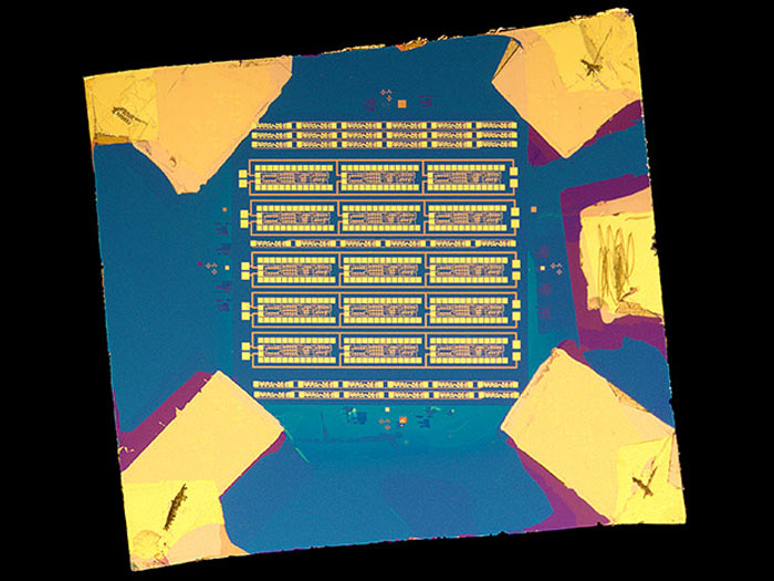
A 1-bit chip with 115 transistors might sound rather anaemic. Nonetheless, the achievement far surpasses previous efforts of circuit making using 2D materials, which have never packed in more than three or so transistors. Study senior author, Thomas Müller (an electrical engineer at the Vienna University of Technology in Austria) admits "our device is of course by no means competitive with current silicon-based microprocessors… it is just a very first step towards a new generation of electronic devices".
There is lots more work to be done in overall development and with yields but the scientists see paths forward. For example, the current molybdenum disulfide films aren't designed for this job and could be made more uniform allowing the scientists to easily "increase the complexity of two-dimensional circuits to tens of thousands of transistors," says Müller. To approach hundreds of millions of transistors in a 2D microchip - as seen in modern silicon chips - chip design will have to switch from NMOS to CMOS, and other 2D materials such as tungsten diselenide might prove to be better semiconductor candidates.
Importantly, the ultimate scaling limit of 2D transistors is estimated to be about 1 nanometer, according to Müller. "This cannot be reached with silicon; the limit there is around 5 nanometers," added the Austrian electrical engineer.