Cutting to the chase: what are the improvements?
Cutting to the chase: what improvements has AMD made with the Radeon HD 5870 and HD 5850?
More powerUnderstanding that GPUs work in a parallel fashion, pushing instructions through a wide architecture, the one obvious method of increasing pure power is to outfit the new design with a greater number of load-handling processors.
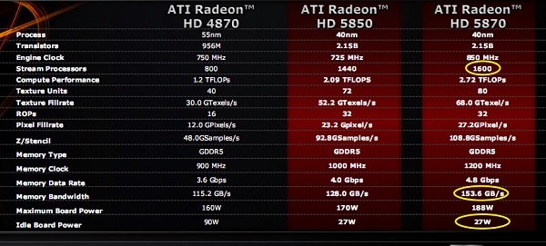
At a fundamental level, this is exactly what AMD has done with the Radeon HD 5870 and HD 5850, as shown by the picture, below.

Image courtesy of AMD
Stream me silly - the balancing act of power vs. cost.
A direct comparison with AMD's single-GPU Radeon HD 4870 shows that the HD 5870 has 2x the number of stream processors, at 1,600, and the trimmed-down HD 5850 some 1.8x, at 1,440.

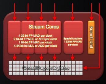
The SP clusters have the same basic setup as on R4K
Increasing the SP count comes at the inevitable cost of die-space. AMD and NVIDIA would dearly love to equip a high-end card with, say, 4,800 SPs, but such a move would cause a) an economically-untenable die-size b) cooling problems associated with the increased transistor count and c) yield problems for multi-billion transistor chips.
In effect, engineering a cutting-edge graphics card is about balancing, as best you can, the competing variables of transistor-counts, heat and power against financial considerations pertaining to pure cost.
Taking the HD 5870 into account, AMD's 'cost' of pumping up the SP count and associated performance-enhancing features is a chip with 2.15bn (billion) transistors, which is more than 2x the previous generation.
AMD's had to move the new GPUs to a 40nm manufacturing process - first tried out on Radeon HD 4770s - to make them economically viable. Even with the significantly smaller process, HD 5850/70's die is 334mm², compared with HD 4870/90's 263mm². They're big, big chips.


