


Concurrent Execution, Caching Improvements
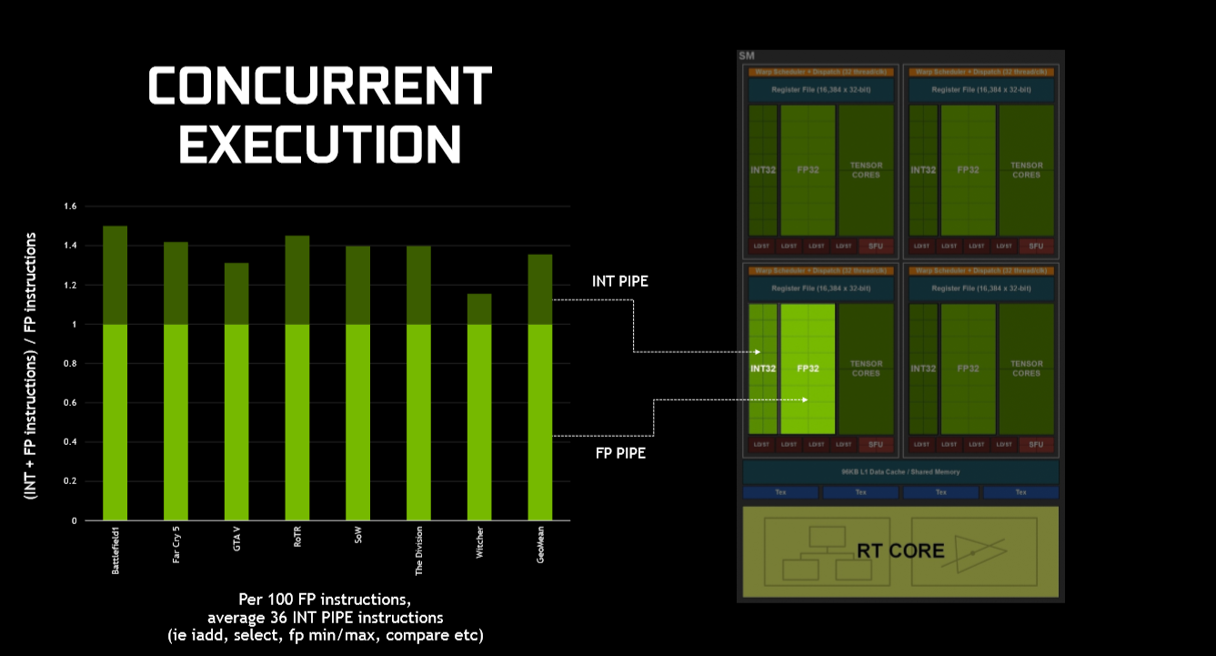
Going back to the adding specific INT32 units, the question then arises as to why you would want to do this and take up valuable silicon space? According to Nvidia, enabling concurrent execution of floating point and integer instructions is a relatively easy way of increasing performance on the code used by today's programs. Looking a broad swathe of modern shader workloads, every 100 floating-point instructions necessitates ancillary calculation of 36 simpler integer instructions, and therefore moving them to a separate block makes sense as it allows the more commonly used FP32 blocks to remain busy doing intensive floating-point work. In Pascal, for example, every time an integer instruction was run the dual-purpose CUDA core couldn't do anything else - it was either floats or integers.
In more detail, a number of applications have to use integer memory address calculations alongside floating-point operations - you can't derive an end result without both being done. These so-called 'inner loop' functions really have to be run concurrently otherwise the GPU encounters that idle time. Nvidia probably wouldn't have bothered with dedicated INT32 processing had the ratio been something like 100:20, but, after having a chat with Nvidia's engineers, it seems as if they had little choice but to add specific units that got around the core-idling problem, first rectified in the Volta microarchitecture. In other words, going down this dual-datapath route enables the FP units to process 36 per cent more throughput than on Pascal. It's all about keeping your execution units as busy as possible.
You can see that each Turing SM is in turn built of four processing engines alongside those RT and Tensor Cores we will talk about later. What's not immediately obvious is what Nvidia has done to the cache allocation and hierarchy within each SM.

Each SM has access to a combined 96KB of L1 and shared memory. The combined and shared - or unified, to put it another way - observations are actually important because it's a fundamental change to how the cache is arranged on Pascal. The reason for this change is to do with how workloads take the best advantage of memory. Nvidia expects graphics workloads to use 64KB for shader memory and 32KB for textures, with the opposite true for compute workloads. It's an either-or kind of problem.
Nvidia further reckons that going down this unified route enables diverse workloads to enjoy fewer cache misses and have lower latency. For example, if a program doesn't use shared-memory cache, then it's pointless devoting 96KB to it, and having a configurable cache makes more sense. Secondly, it makes programmers lives easier as applications have to be tuned specifically for shared memory whilst L1 cache is accessed directly.
This Turing cache arrangement is clearly designed to minimise the bottlenecks that have been identified within Pascal, and it's no coincidence that Volta, the intermediate architecture, uses this shared approach, too.
Adding to this configurability is the effective doubling of caching speeds for both L1 (through being part of the shared-mem block) and L2, while the latter is also doubled in size. This combination ought to result in less off-chip traffic, which is always a good thing.
Point is, each change - shader-core and caching - is in direct response to how Nvidia has seen workloads develop since the time that the Pascal design was put to bed.
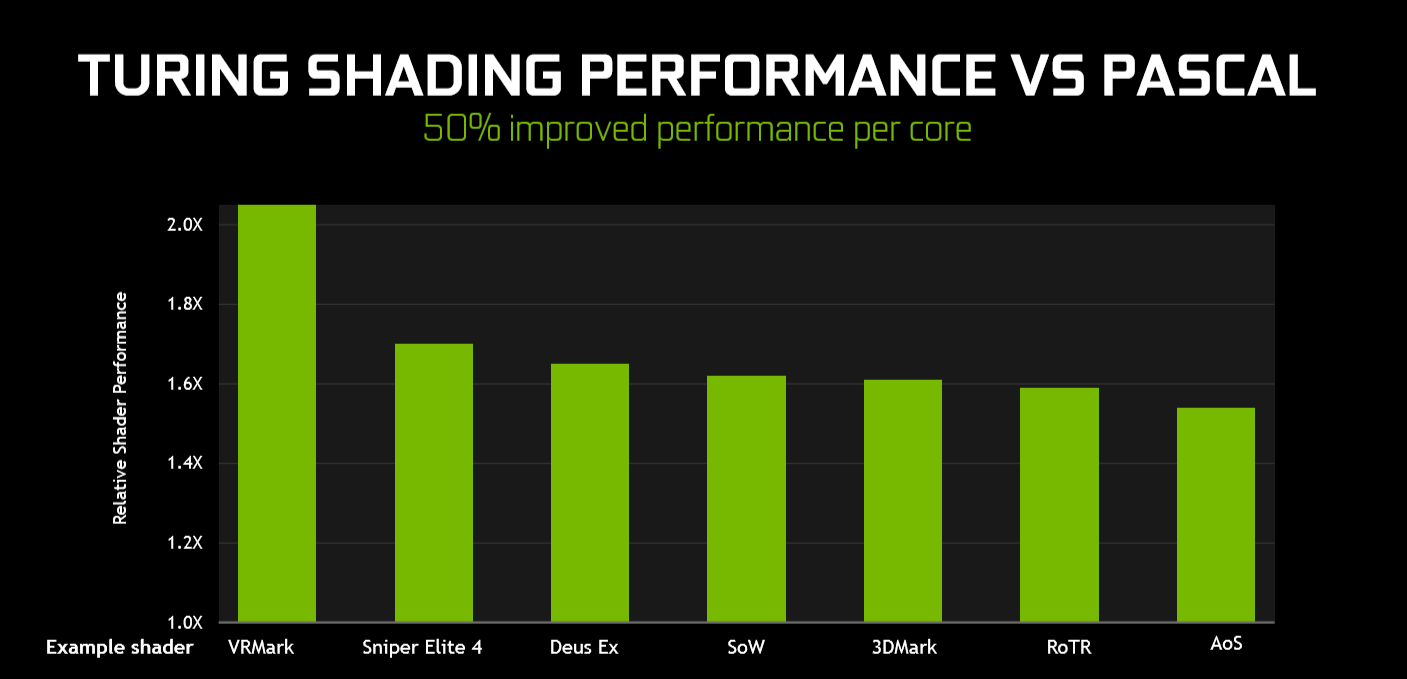
The sum benefit of having concurrent integer instruction execution, a smarter cache mechanism, and a number of minor tweaks that are outside the remit of this piece to cover, is approximately 50 per cent more shading performance per core, so not only does Turing have more cores to play with, they do more work per cycle. One architecture's FLOPS don't work the same way as another's, clearly.


