


Introduction and Architecture
Today, July 7, is a busy and important day for AMD. The Zen 2 CPU and Navi GPU architectures are officially released to retail in the form of the Ryzen 3rd Gen processors and Radeon RX 5700/XT GPUs. In this review well be focussing on the CPU releases, so head on over here for an in-depth review of the new graphics, compared against Nvidia's recently-released RTX Super cards.
It is meaningful to under the upcoming benchmarks with solid knowledge of what Zen 2 brings to the table, how it is better and more efficient than its Zen and Zen+ predecessors powering Ryzen 1st and 2nd Generation chips, respectively, and how well it compares against Intel's premium mainstream chips in a wide range of benchmarks.
Zen 2 - Building on momentum
First off, Zen 2 is an evolution of first-generation Zen rather than a grounds-up design. This makes implicit sense because AMD made a clean break with Zen compared to the maligned Bulldozer/Excavator core.
Evolutionary designs enable engineers to pick off all the low-hanging fruit missed first time around, iron out bottleneck kinks, and then focus on laying down transistors that enhance performance.
Zen 2, which began life in mid-2015 according to CPU chief architect Mike Clark, was designed primarily to boost the all-important instructions per clock cycle (IPC) metric which historically has been lacking on AMD chips when compared directly to Intel. IPC has become more important as liberal increases in frequency have dried up: reliably hitting 5GHz on any modern processor is difficult.
AMD claims Zen 2, whose execution cores are hewn from a leading-edge 7nm process, increases IPC by a full 15 per cent compared to original Zen, which is impressive given the base architecture is familiar, and that's without taking any additional frequency headroom into account.
Improving the front-end - deeper and smarter
Whether you are designing for an ARM core or high-performance x86, as in this case, there are a number of techniques that CPU architects adopt in order to enhance IPC. It all starts off at the front-end of the core with the branch-prediction unit. Having excellent accuracy here - knowing with near-perfect certainty which way branches are going to go - enables fewer pipeline misses, conserves power, and fundamentally powers the execution cores. A CPU architect spends an inordinate amount of time at this stage because it sets the scene for everything that follows.
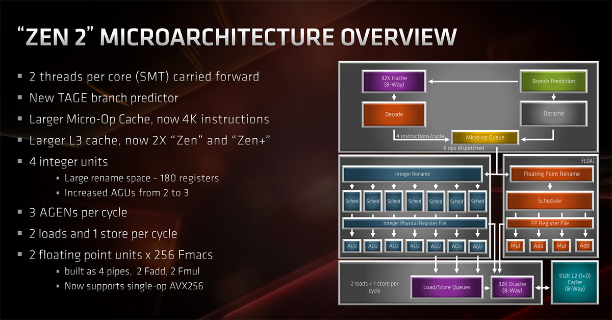
Zen 2 uses what is known as a TAGE branch predictor that carries a deeper branch history than its predecessor. This is augmented by larger branch-target buffers (BTB) than Zen (+), with a doubling of the L1 BTB (512 entries) and almost-double L2 BTB (7K now). The theme of larger is better continues with the MOP cache growing to 4K. This is especially handy because no processor wants to decode complex operations multiple times. Decoding them once and putting them into a large(r) cache speeds things up and makes the processor more efficient because it can bypass the decode stage if the same micro-op is required later on.
In an interesting move, after analysing numerous applications and their dataset size, the instruction cache actually drops from 64KB to 32KB but increases associativity from 4-way to 8-way. The reason is that, according to Mike Clark, this reduction barely reduces performance: most datasets need way more than 64KB anyway. The new cache features improved prefetching and better utilisation, too. What all this means is that Zen 2's front-end is more efficient - helping IPC - but does come at the cost of taking up a bit more space.
Wider execution and, finally, true AVX256
Looking midway down, into the guts of Zen 2, shows that AMD maintains the four ALUs of Zen but adds a third address generation unit (AGU) for accelerating the calculation of memory addresses needed before grabbing data from memory. As usual, more is better in most cases, and Zen 2 backs this up by increasing the integer rename space from 168 to 180 registers. Put simply, Zen 2 has more ALU capability than Zen(+), and is able to issue seven per clock cycle, up from six.
AMD also recognised that while the floating-point potential of Zen was rather handsome in real-world instances, it needed to beef-up the AVX capability by going wider. This is why, thanks to 256-bit registers, it is able to now process double-wide AVX256 in one clock cycle, double that of original Zen. This is important because it's one area where rival Intel has always enjoyed a decent lead, shown in well-tuned content-creation applications.
Cache is king
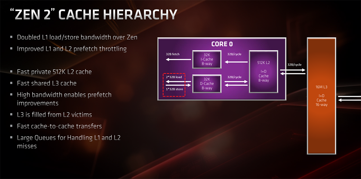
In common with previous designs, each of Zen 2's cores features 32KB of L1 D-Cache, whose load/store bandwidth is doubled this time around by jumping from 16 bytes to 32 bytes. Handy for keeping as much data on chip as possible. Per-core L2 cache is kept at the same 512KB.
Four cores are grouped into what is known as a CCX and each four-core group has access to L3 cache. For Zen 2, the big change is that each CCX's L3 cache is doubled, from 8MB to 16MB, and you'll see the sum of L2 and L3 cache known as GameCache in AMD marketing.
And it's this combination of keeping as much data on-chip as possible, having a smarter front-end, wider execution unit, and enhanced floating-point capability that combine to offer more IPC than on previous iterations of Zen. The exact gain is dependent on how diverse workload benefits from each of these performance-adding features - some respond excellently to heaps more cache and associated lower average latency, others to floating-point, but in every case Zen 2 ought to be faster than Zen(+) on a clock-for-clock basis.
There is, however, another manifest reason why AMD has gone L3 cache-heavy. It's to do with how Zen 2 is constructed. More precisely, the nature of the flexible chiplet design.
Chips, chiplets, PCIe 4
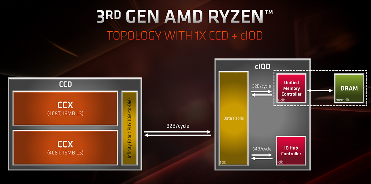
Fabrication is a horribly expensive business. You only want your most cutting-edge technology to use the latest processes, yet the nature of a modern CPU, which is verging on being an SoC more than a pure serial processor, is that you don't need the I/O, memory controller, PCIe, and so forth, to be on the same process. Splitting it out into its own block makes sense because it can reduce cost - by using older, more mature fab processes - and also provide an extra level of flexibility. This is AMD's thinking with the chiplet design.
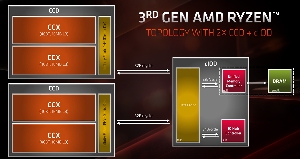
The above graphic illustrates how Zen 2 makes the CCXs independent of the I/O block. It shows a couple of CCX complexes lashed together via Infinity Fabric to create an 8C16T chip complete with 4MB of L2 and 32MB of L3 cache. This modular CCD is then connected to the I/O chip (cIOD) via a high-speed data fabric capable of reading 32 bytes and writing 16 bytes on each clock cycle. That may cause a problem for the memory write speeds when using processors equipped with single CCD - any Ryzen 3000-series with eight or fewer cores - because the data fabric-to-UMC speed, inside the cIOD, is 32 bytes for reads and writes: they don't match.
AMD says that this is a calculated design choice for Zen 2, due to most client workloads not writing as much. Halving the data link write speed between CCD and cIOD saves area, improves power, and has ancillary knock-on benefits, too. The downside is half-write speed because of the slowness of the data fabric in that direction.
The key takeaway is that, because of its relative simplicity, the I/O block can be produced on an older process. That's exactly the case, as while TSMC is the go-to solution for the CCD silicon, GlobalFoundries' 12nm node provides the silicon backbone for the I/O.
The beauty is that, should AMD want more cores and threads for a particular segment, a second 8C16T CCD can be further added and connected to the I/O via the same high-speed link. This is the case with all >8-core Zen 2-based CPUs..
The I/O block itself carries the dual-channel memory controller, which has been upgraded and optimised for Zen 2 to run at much higher speeds - an Infinity Fabric divider comes in at 3,733MHz; AMD reckons the controller will do well over 4,000MHz - and offers 16 lanes of PCIe Gen 4 for graphics, four PCIe Gen 4 for NMVe/SATA drives, and a further four same-spec lanes for connecting to the chipset. It also features four USB 3.1 G2 ports, and other associated I/O goodies.
The way in which Zen 2 is designed means that each CCX's average latency to main memory is about the same, irrespective if you have one, two, or four CCXs active. Back on point, having 16MB of L3 cache per CCX helps mitigate against moving the I/O functions over to a separate, distinct block - it's a necessary evil of going down a chiplet architecture.
Size matters - the power of 7nm
You would think that having a wider execution core, larger caches in general, and a massive 16MB of L3 would cause each of Zen 2's CCX's to balloon in size compared to Zen. That would be the case, one would think, if AMD stuck to the 14/12nm processes of Zen and Zen+, respectively. The kicker is that AMD has been able to lay down Zen 2's undeniably bigger transistor floor plan whilst decreasing the silicon area by almost half.
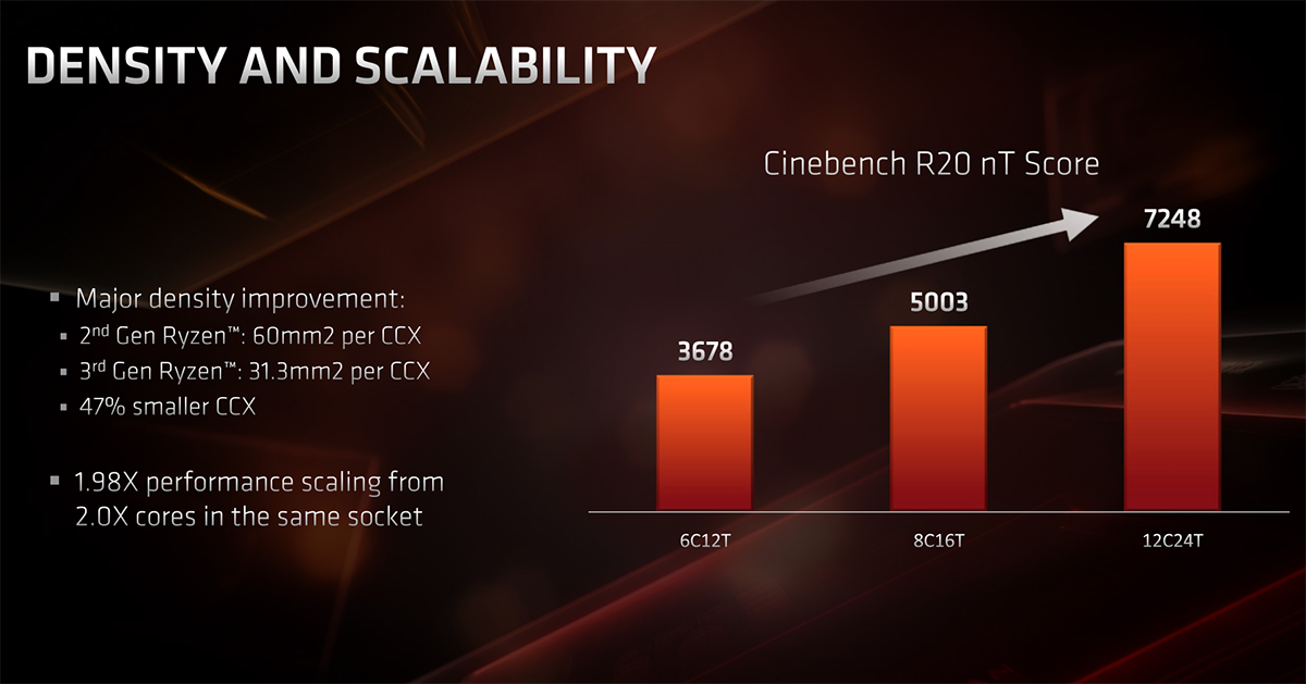
How? That's the special density sauce heralded by producing the CCX's on a leading-edge 7nm process from TSMC. Even with the larger design and cache footprint, AMD reckons that each of Zen 2's CCXs takes up just over half the space of Zen. There's a little more to it than that, because each dual-CCX CCD has a few extra bits of silicon (Infinity Fabric) that takes it up to 74mm², yet there's still clear advantage in going down the cutting-edge route.
AMD chief CPU architect, Mike Clark, alluded to initial concerns that chasing double-digit IPC on Zen 2, combined with the complexity of the 7nm process, plus the need to rein in voltage, could lead to per-core frequency dropping between generations. Not such a big deal in the server world where extra cores and threads can make up the shortfall, but certainly a consideration in the client space.
Through some clever power management and work with TSMC, the EDA tool guys, and modelling, Zen 2, productised as Ryzen 3000-series, runs faster than the previous generations, too.
So, now that we have a firm grounding into how Zen 2 is built, and why it is better from an IPC, flexibility, and footprint point of view, let's now see how the various models stack up.


