Alder Lake's Golden Cove
It's shaping up to be a busy autumn for Intel. Most pertinent for the PC enthusiast community is the release of next-generation processors built on the all-new Alder Lake architecture.
Alder Lake is especially interesting as, unusually, it is coming to desktop first, followed by mobile and server implementations in the early part of 2022.
Intel took further wraps off the nuts and bolts during this week's virtual Architecture Day, which also encompassed some interesting details about discrete gaming GPUs (Intel Arc), server processors (Sapphire Rapids) and the AI monster that is Ponte Vecchio. We'll cover those announcements separately.
Back on track to Alder Lake. We already know a fair bit about it from voluminous rumours, and most of them are on the money. To be productised as Intel 12th Gen Core, Alder Lake will arrive in late October in multiple TDP configurations consistent with the present generation.
Going from the outside in, Alder Lake chips are built on what is now referred to as the 'Intel 7' process. Previously known as 10nm Enhanced SuperFin (ESF), Intel says the new process nomenclature is more comparable with the competition. The key difference is how Intel goes about building these chips. As you may already know, they use a hybrid architecture that mates Golden Cove 'Performance' cores with power-optimised Gracemont 'Efficient' cores for improved multi-threading and performance-per-watt metrics, the company says.
Let's focus on the larger, more powerful Golden Cove core and implementation first as we know more about it.
Announced at Architecture Day 2020, Golden Cove is the direct successor to mobile Sunny Cove and desktop Cypress Cove, with the latter being a 14nm backport for the 11th Gen Core desktop processors. An interim design, Tiger Lake, based on the Willow Cove architecture, is available for mobile only.
Golden Cove is a logical progression over previous Coves and takes in bits from both Sunny and Willow. This is not an all-new architecture, mind, as Intel has effectively reworked existing designs to extract more performance through compute parallelism aided by larger, faster caches, deeper queues and new extensions for burgeoning AI workloads.
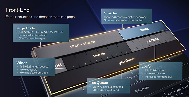
On the front-end, Intel thinks it is worth devoting die space and power to beefing up the performance. Makes sense when you're feeding a more capable execution engine. Of particular note, the micro-op cache, used to store already-decoded instructions, is increased to 4K and hands off eight micro-ops per cycle, compared with 2.25K and six from Sunny Cove. This means the processor spends less time having to decode them again which naturally aids performance for reused information. In concert with this, the design can fetch and decode on a 32-byte window, doubling Sunny Cove. All of this costs die-space resource but is, through simulation, worth it in feeding the stronger out-of-order execution engine.
Intel says it has noticed that applications' code footprint is increasing at a rate fast enough to swamp previous architectures. This is why Golden Cove pays special attention to this facet and duly doubles the 4K pages stored in the translation buffer and increases the branch target buffer from 5K to 12K, which is handy for code-heavy workloads. What's cool here is that, according to Intel, it uses machine learning to dynamically adjust its size to save power. This improvement is forced upon Intel as a direct result of emerging workloads.
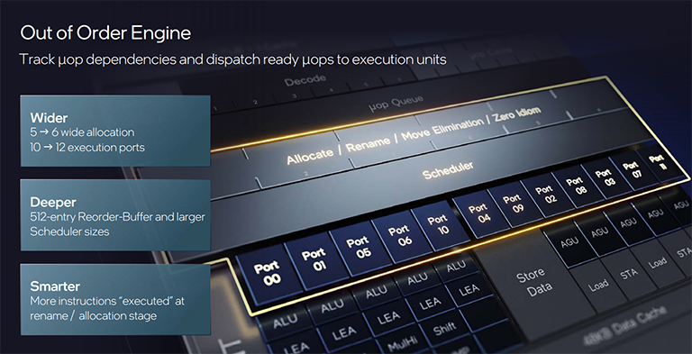
Golden Cove does to Sunny Cove what it does to Skylake. By that we mean it increases instruction allocation width (from 5 to 6) and execution ports (10 to 12). Further key call outs are adding a fifth ALU and fifth single-cycle LEA for enhanced integer processing, which remains a mainstay for a lot of code.
It would have been handy for Intel to provide a block diagram of Golden Cove, but nonetheless, the Vector portion gets three-cycle faster adders on ports 1 and 5. Why? Because on Sunny Cove the same floating-point-add operations are done on the FMA cores and with higher latencies. Golden Cove's FMAs now support FP16 which is useful for, say, networking operations. These tweaks again represent Intel attempting to deliver the best cross-segment architecture for use-cases in 2021-2023.
The memory subsystem, meanwhile, is notable for getting more L2 cache per core - 1.25MB vs. 512KB, so same as mobile Tiger Lake - alongside greater efficiencies in the store/load mechanism through deeper buffers. Moving to AI for a second, Intel massively boosts INT8 processing - the instruction bedrock for AI - from 256 to 2,048 operations per cycle. How? By implementing Advanced Matrix Extensions (AMX). This technology will be detailed later and is of more import to datacentre Xeon chips.
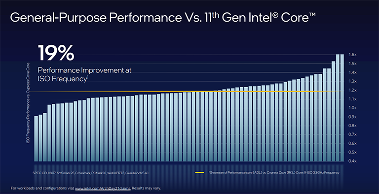
Really, if all of this sounds overly complicated and the numbers and techniques make little sense, understand that Golden Cove's extra buffers, execution units, ports, et al, are all designed to improve the core's instruction-per-clock (IPC) throughput for today and tomorrow's workloads. Intel sees these changes as the most optimal way of increasing IPC; AMD does things differently. The sum of this engineering is around 19 per cent IPC improvement across a broad swathe of applications. Newer or emerging workloads tend to see higher gains as the architecture employs dedicated hardware (think AI) and older code probably a bit less.
Golden Cove, therefore, represents the same kind of performance jump that we saw from Skylake to Sunny Cove, and a 19 per cent IPC improvement is nothing to be sniffed at.
Yet Golden Cove is not the most interesting part of the design. Remember how Alder Lake is a hybrid design? The other part is the introduction of smaller, power-efficient cores known by the codename Gracemont and referred to as the Efficient part of CPU the SoC.


