


A brief reference look
We'll take a quick look at the reference board from VIA. Don't expect any daring design.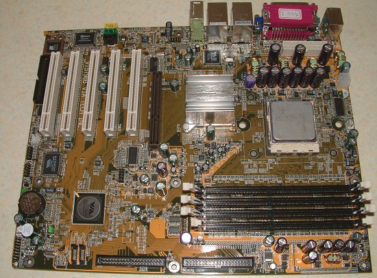
It's a little less reference than most other VIA boards. You can actually install this into a regular case. VPSD, VIA's Platform Solutions Division, have marketed VIA-branded boards before. The K8T800 Pro seems a likely candidate for such a role. Anyway, this S940 board supports both AMD FX and Opteron CPUs in a single-CPU setup. That also entails dual-channel RAM support. Two channels are created by housing DRAM modules in either the uppper or lower DRAM slots. Of course, one can still run in DC mode with all slots populated.

A shiny passive heatsink is enough to keep the northbridge cool. The heatsink did become hot after prolonged use, but system heat didn't impact on stability. The reference board didn't crash once during a weekend of testing. We must note that there's not a whole lot of difference between the Pro and non-Pro models, so stability is expected to be good.
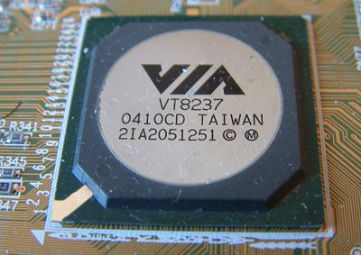
As you'd expect, it's a VIA benefit right across the board, from discrete FireWire support to LAN duties. VIA's one of the very few firms that doesn't have to look elsewhere when bumping up the features' count. The block diagram on the previous page shows off VIA's new VT8251 southbridge. VIA's reference model uses the tried and trusted '8237. That means on-chip SATA support at the very least. As you are beginning to see, the K7T800 Pro is a minor enhancement over the incumbent model.
We'd expect motherboard manufacturers to go with the kind of layout VIA has done here. There's plenty of component action, thanks to a number of discrete controllers required to make up for the features' shortfall in the '8237, yet VIA's laid them out sensibly. If this was a production motherboard from, say, ASUS, it would get reasonable marks for layout.
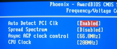
There's nothing much that grabs the eye in the BIOS. The only way to definitively state that this is a Pro board is through a 1GHz HyperTransport link (not shown) and the ability to run asynchronous clocks for the AGP And PCI buses. It's a shame, then, that the reference board doesn't allow multiplier adjustment. Just how useful is a locked bus, in the context of overclocking, when the CPU maxes out at around 214MHz driven clock?. What's needed is a drop in multiplier and increase in driven clock speed. Something along the lines of 9x250MHz, ideally.


