|
Lets get right into the thick of things with Intel's official chipset diagram.
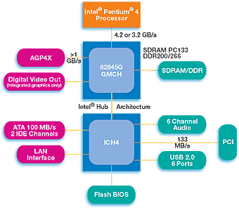
Starting with the link from CPU to northbridge or Graphics Memory Controller Hub (GMCH) as Intel likes to call it, we can see that the northbridge has had quite a bit added to it since the original inception of the chipset. Like i845E, the chipset now officially supports the new 533MHz (133QDR) processor front side bus and can theoretically supply the processor with 4.2GB/sec of memory bandwidth in that configuration.
You'll also notice from the moniker, GMCH, that the bridge also has an integrated graphics controller. If you follow the industry at all, you'll know that onboard graphics solutions at the present time by their very design, will never be as quick as a dedicated graphics controller. Mainly as a nod to the business market, i845G was designed to allow board makers to offer entire solutions on their motherboards with only memory, a CPU and a storage device needed to complete a fully working system since most i845G boards will ship with Ethernet and audio controllers on board too.
In terms of pin count and package, the GCMH runs to 760 pins and is manufactured using a FCBGA (Flip Chip Ball Grid Array) package type.
Hosting the memory controller and AGP interface along with the graphics controller, the GMCH is responsible for the primary functions on the chipset. The memory controller officially supports up to DDR266 memory, however you may see a few i845G/E boards offer up 4:3 memory multiplier ration (1.33 x front side bus) for pseudo-DDR333 support. Being 1.33x, the final memory speed at 533MHz (133) front side bus is 354MHz, not the 333MHz needed for proper DDR333 support. So make sure your memory can handle 354MHz at 133MHz front side bus if you wish to use PC2700/DDR333 memory with your i845G/E board.
The AGP controller is Intel's standard AGP controller as seen on other Pentium 4 chipsets. Supporting onboard graphics, the chipset also supports a DVI riser board to be present in the AGP slot to provide digital output along with the DB15 output that replaces a serial port for analogue output. DFI kindly ship the DVI riser with their NB76-EA board but not the NB76-EC and you may find that other manufacturers don't ship it either.
Using Intel's Hub Architecture, the GMCH links to the southbridge with a bus much like VIA's V-Link or SiS MultIOL.
The southbridge or I/O Controller Hub (ICH) is Intel's ICH4 implementation. Handling the PCI and other peripheral bus interfaces, the ICH4 is Intel's current flagship southbridge. While it wont officially support ICH4 with i850/i850E, the new bridge is officially compatible with the i845G/E northbridge.
A standard 133MB/sec PCI implementation is present, brought from previous chipsets along with ATA100 support on the IDE controller. Note the bridge doesn't support ATA133 as you may see elsewhere and there are also some not so well known issues with IDE write performance in the ICH4 which we'll save for another article.
USB2.0 (6 ports), AC97 audio and an Ethernet interface round off the ICH4 bridge and the chipset as a whole. Basically an upgrade to 533MHz front side bus processors paired with the ever popular ICH4 bridge and an integrated graphics core are what we have with i845G.
So what about boards based on it and more specifically DFI's implementation in the form of the NB76? Lets take a look at the board itself.
|


