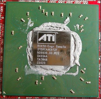
RV410 versus R420 and R423
For this comparison, I'm comparing the X700 XT version against an X800 XT Platinum Edition (R420) and X800 XT (R423), so you can get some indication of the differences in the high-end mid-range and high-end high-end parts that ATI produce. Obviously, X800 PRO sits somewhere in between.
Click for a bigger version
| RV410 | R420 | R423 | |
| Process | 110nm @ TSMC | 130nm @ TSMC low-k | 130nm @ TSMC low-k |
| Transistor Count | Unknown | Unknown | Unknown |
| Geometry Pipeline | VS2.0 + VS3.0 geometry instancing support | VS2.0 + VS3.0 geometry instancing support | VS2.0 + VS3.0 geometry instancing support |
| Fragment Processor | PS2.0b | PS2.0b | PS2.0b |
| Fragment Processor Setup | 2 full (vector/scalar) ALU (not equal), one texture ALU, F-buffer | 2 full (vector/scalar) ALU (not equal), one texture ALU, F-buffer | 2 full (vector/scalar) ALU (not equal), one texture ALU, F-buffer |
| Fragment Processor Precision | FP24 | FP24 | FP24 |
| Traditional Render Setup | 8 x 1 | 16 x 1 | 16 x 1 |
| ROPs | 8 | 16 | 16 |
| Vertex Shaders | 6 | 6 | 6 |
| Basic Texture Filtering | Bilinear | Bilinear | Bilinear |
| Texture Filtering | Bilinear, Trilinear, 16X Anisotropic | Bilinear, Trilinear, 16X Anisotropic | Bilinear, Trilinear, 16X Anisotropic |
| Antialiasing | Multi-sampling | Multi-sampling | Multi-sampling |
| AA Sample Type | Ordered grid, multiple sample grids, up to 6X, up to 3X temporal | Ordered grid, multiple sample grids, up to 6X, up to 3X temporal | Ordered grid, multiple sample grids, up to 6X, up to 3X temporal |
| Native Bus Support | PEG16X | AGP8X | PEG16X |
| Memory support | GDDR3 | GDDR3 | GDDR3 |
| Basic Core Frequency | 475MHz | 520MHz | 500MHz |
| Basic Memory Frequency | 1050MHz | 1120MHz | 1000MHz |
| Memory Bus Width | 128-bit, memory crossbar | 256-bit, memory crossbar | 256-bit, memory crossbar |
| Basic Pixel Fillrate | 3800Mpixel/sec | 8320Mpixel/sec | 8000Mpixel/sec |
| Basic Multitexture Fillrate | 3800Mtexel/sec | 8320Mtexel/sec | 8000Mtexel/sec |
| Basic Memory Bandwidth | ~16.80GB/sec | ~35.84GB/sec | ~32.00GB/sec |
RV410 is ATI's first mid-range part that's produced on TSMC's 110nm foundry process. A smaller foundry process means a smaller die size for the same transistor count. With RV410 having significantly less transistors than R420, due to half the fragment pipes, half the ROPs and a smaller memory bus width, RV410's die size and transistor count is significantly smaller than R420 in both respects, crucial for a mass-market part in this sector.
That ATI didn't chop anything from the Z-buffer optimisation scheme present in R420 is perhaps the most significant part of RV410's design. ATI's previous RV parts have removed the heirarchical Z-buffer from the full, parent R part. Not so in this case, allowing RV410 to have maximum efficiency after the geometry setup engine, discarding pixels before they enter the fragment shaders, as possible.
Unlike NV43, RV410 keeps one ROP per fragment pipe, whereas NVIDIA's mid-range GPU cuts that in half, limiting its raw, single textured, bilinear filtered pixel fillrate. So RV410 has the edge in raw pixel output at the same clocks, compared to NV43.
RV410's vertex shader unit count is surprising too. It retains the same VS unit count as R420 and R423, giving the X700 XT at 475MHz the same vertex shader power as an X800 PRO. So at the same clocks, RV410 has roughly twice the vertex shader power as NV43. In games that are geometry or vertex shader limited, that could be significant.
A 128-bit memory bus width, combined with the same fast memory types that R420 and R423 support, means that RV410's memory bandwidth requirements are balanced when compared to the fragment shader and ROP output.
Native PEG16X bus support without a bridge chip, like NV43, means that RV410 will make its deput on PCI Express first, with an AGP variant (native interface again, no bridge chip, probably called RV413 or somesuch) coming later.
RV410's rendering pipeline
RV410's render pipeline is pretty simple to imagine. Much like NV43, RV410 generates geometry using the vertex shader, either by running a vertex program or emulating a fixed function path from hardware and Shader Models of old. That geometry is sorted for depth, the Z-buffer and its optimisation scheme compressing and disregarded vertex data early in the pipeline to stop geometry being turned into data that needn't be processed, and if it does need to be operated on, that it's optimised as much as possible for the next part of the pipeline.Vertex data is tranformed into pixel fragments and dispatched to the fragment shaders by the GPUs scheduler. The fragment shaders operate on the pixel fragments in parallel as much as possible, optimising data throughput, getting as many fragments through the pipeline as possible. The fragment shaders, as described in the table above, are made of two functional arithmetic units (vector and scaler units, not equal in capability, the 2nd unit with undisclosed ability), a texturing unit, able to supply fragment programs being run with data from a texture source, with the F-buffer able to loop fragments back round the fragment shader units with saved state, unlimited times.
After processing in those units, the output fragments are passed into a crossbar dispatch unit, which feeds them into the GPU's ROPs (render output units), that do all the blending, combining, anti-aliasing and colour compression of the output buffers, before the final processed pixels are spat out for display.
It's not too hard to understand. Generate triangles, convert them to pixels on the screen, run your shaders that change their appearance, output the fragments and do anti-aliasing and buffer combining and blending, draw the pixels on your screen. Et voila (simplified somewhat).


