


NVIDIA GeForce 7950 GT
NVIDIA dropped the reference board by this time, letting us check out their new cooler revision in action at the same time as we checked out the board's performance.
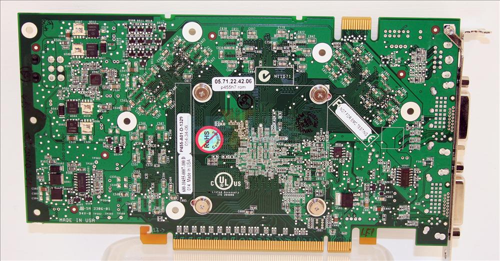
Check out the bigger version of the first picture (clickety click) and you'll see the Infineon DRAMs. Usual suppliers Samsung don't make the grade this time, NVIDIA choosing the HYB18H512321AF-14 devices instead. Obviously 512Mib in density, each, and rated at a 1.4ns refresh cycle, that's ~715MHz or so. NVIDIA run them at 700MHz of course.
The PCB is nothing we haven't seen before, NVIDIA asking that you connect up an external power connector when you use a 7950 GT, as all 79xx products have before it. Despite just a regular power and ground connection for fan power, NVIDIA certainly do get away with calling the cooler revised, the board making much less noise than your author remembered older 7900 GTs making. Indeed, I ran back-to-back tests with 7900 GT and 7950 GT to check.
Both DVI ports are dual-link capable and support HDCP. AIB partners can't wiggle out of that either, all 7950 GTs from all partners supporting the copy protection standard on both ports. We didn't check on the HDCP support but we did hook up a Dell 3007 WFP to the board's ports (both of 'em) to make sure the dual-link was working, and it was.
You can SLI a pair of them if you feel frisky and with single-slot coolers you might even get away with doing so in smaller form factor systems. Power draw we figure to be around 85W or so, depending on load condition, although we can't be 100% conclusive. Shame NVIDIA didn't sample two, we'd have been able to check on that a bit better, but we're sure we're not far off.
It slides into a VLB slot on your Intel 486 DX-based system......sorry, PCI Express slot on your modern PC system, and that's pretty much it in terms of physicals.
Chips and clocks and FLOPs and ROPs
Theoretical figures look like this.| Theoretical Rates for GeForce 7950 and 7900 GT | ||
|---|---|---|
| NVIDIA GeForce 7950 GT | NVIDIA GeForce 7900 GT | |
| Core Clock | 550MHz (550MHz VS) | 450MHz (470MHz VS) |
| Memory Clock | 700MHz | 660MHz |
| Pixel fillrate | 8.80G pixels/sec | 7.20G pixels/sec |
| Texture sampling rate | 52.8G samples/sec | 43.2G samples/sec |
| Z-only rate | 17.6G samples/sec | 14.4G samples/sec |
| Vertex transform rate | 1.10G tris/sec | 0.94G tris/sec |
| VP MADD issue rate | 4.40G instr/sec | 3.76G instr/sec |
| FP MADD issue rate | 26.4G instr/sec | 21.6G instr/sec |
| Memory bandwidth | 44.80 GB/sec | 42.24 GB/sec |
A 22% increase in basic GPU rates is partnered by a more modest 6% rise in memory bandwidth. We saw in the analysis of 7900 GS that 7900 GT in default configuration is bandwidth starved at interesting resolutions, so that 6% increase should translate well. At 650/800MHz though, GeForce 7900 GTX remains a very useful cut above either GT on paper, so the comparison will be interesting.
Also remember that 7950 GT doubles the on-board memory size compared to what it replaces, sporting 512MiB of GDDR3, not 256MiB. The situations where that'll help are simple to imagine.


