|
The easiest way to grasp the difference between the two implementations (remember, Radeon 9500 is an R300 chip just like in Radeon 9700, just a difference implementation of it) is with numbers. Straight comparison between the two in handy table format should suffice.
| Radeon 9600 Pro | Radeon 9500 Pro |
| |
|
RV350 |
R300 |
| Transistor count |
Unknown |
110 million |
| Manufacturing process |
130 nanometre |
150 nanometre |
| Pixel pipelines |
4 |
8 |
| Pixel shader units |
4 |
8 |
| Memory bus width |
128-bit/16-byte |
128-bit/16-byte |
| Texturing units |
1 |
1 |
| Core clock |
400MHz |
275MHz |
| Memory clock |
600MHz DDR |
540MHz DDR |
| Pixel fillrate |
1600 Mpixels/sec |
2200 Mpixels/sec |
| Texture fillrate |
1600 Mtexels/sec |
2200 Mtexels/sec |
| Memory bandwidth |
~9.60GB/sec |
~8.64GB/sec |
|
|
So what's the quick verdict from the data in the table above? More core clock frequency to make up for the pixel and texel fillrate disadvantage that comes from running half the render pipes. That also means half the shader power at the same clocks so more core clock helps make up that defecit too.
We've got 60MHz more on the memory but the bus width is the same so there's no massive increase in raw memory bandwidth. What the RV350 does do differently to R300 in this regard is more effeciency, especially with Z-buffer operations. Without going in to too many specifics, RV350 can do up to 8:1 Z-buffer compression compared to 6:1 max on R300. There's also a slight advantage over the 128-bit memory bus R300 due to the fact that RV350 was designed for that bus width from day one. No disabling half the memory controllers this time.
That also means that since the RV350 is fixed in this regard, 4 render pipes and 1 texture and shader unit per pipe and a fixed memory bus width, there will be no magic software or BIOS hacks to enable another 4 pipelines like with R300 based Radeon 9500's. They just simply aren't there, a free performance lunch in that regard isn't doable this time around.
Also, although it doesn't matter much, there's no infinite instruction length for the shader units like with Radeon 9800 Pro. R350's F-buffer for this isn't carried on to RV350. But it's not a big deal, there are no DX9+ games available that need more instructions in their shaders than DirectX 9 calls for, or indeed provides.
So does the core clock increase, and it's a fairly hefty one, keep pace with the outgoing Radeon 9500 Pro despite its processing power handicap at the same clocks? We'll have to benchmark it and see.
Lastly, the process shrink from 150nm to 130nm means less voltage to operate at the same clocks so it might possibly be easier on your electricity bill, even at 400MHz. It also means overclocking it should be fun. We'll get to that later.
I could rabbit on about shader power and how a 4x1 pipeline/texture unit layout is fine for todays games but you don't need to hear that now, we can cover it during the benchmarks. Let's take a look at some pictures instead.
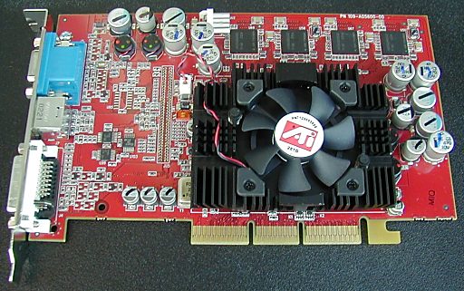
 Radeon 9500 Pro (picture blatantly stolen from the Tech Report)
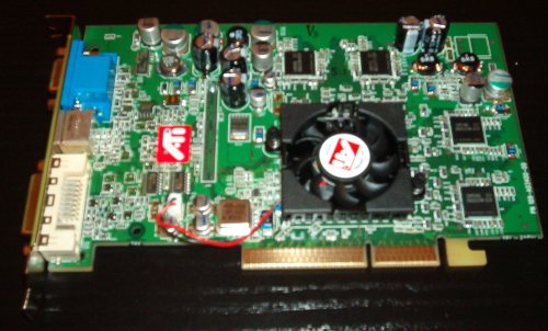
 Radeon 9600 Pro
As you can see, Radeon 9600 Pro has a different PCB to Radeon 9500 Pro and doesn't require any auxiliary power (yay!). The Radeon 9600 Pro PCB resembles 9700 Pro in terms of memory chip placement and Samsung get to take care of memory duties once again.
The card sports the regular VGA, S-Video, DVI-I backplane arrangement and the DVI and S-Video ports share a display unit on the card so dual head operation is limited to VGA and DVI, or VGA and S-Video. Of course, can run the card in Theatre mode where any hardware video overlays, as used in video display, are automatically dispatched to the TV head and run full screen and hardware accelerated.
You have adjustment over the aspect ratio from the driver for those awkward videos and the driver exposes a full MPEG-2 decoder to the operating system for full DVD and other MPEG-2 video acceleration.
So what about performance?
|