


GPU Communications Scheme and Physicals
I mentioned in our preview of G71 and G73, here, that NVIDIA's new 90nm GPUs have a pair of SLI interfaces. NVIDIA implement a number of repurposable interfaces on their GPUs, for anticipated I/O. Previous thinking had them abusing the VIP (video input port) for their SLI connection in first generation SLI, but it transpires that they're just appropriating one of the general I/O interfaces to create the 2nd interface present on the new chips.Along with each new chip containing two SLI interfaces, the interfaces can also accept antialiasing sample data, for accelerating SLI AA modes. Here's how the GPUs communicate, forgive the rudimentary diagram, and find an even simpler one here.
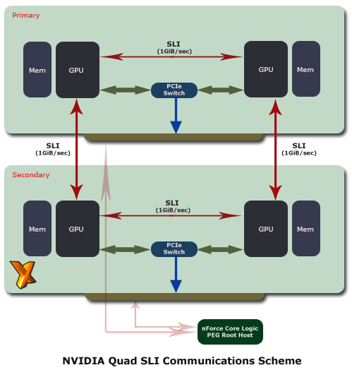
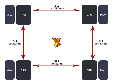
Much like the HyperTransport communications scheme between AMD Opteron processors in a multi-CPU system, Quad SLI uses a ring-like topology to connect GPUs as they communicate. If we call the two GX2 boards represented in the diagram A and B, and their respective GPUs 1 and 2, you get the following links: A1 to A2; B1 to B2; A1 to B1; A2 to B2.
Those links are discrete and the 1GiB/sec comes from an 8-bit link at 1GHz (the similarities to HyperTransport run to more than the topology!).
GPUs on a GX2 communicate over PCI Express (for OOB comms that can't go over the SLI links) via a PCI Express switch. The switch has a 48-lane internal bandwidth which works out at a 16-lane link for each GPU, with the last 16-lane link to the slot. The switch will act as a multiplexer mostly, although that does depend on the rendering mode. Data bound for both GPUs on a GX2 will be collected by the switch device and sent to the right PCB, and return data will be multiplexed onto the bus.
The nForce core logic is the final arbiter of bus data allowing the whole thing to work properly.
Physical Bits
If you examine a GX2 board closely you can see the inter-PCB links for SLI and PCI Express.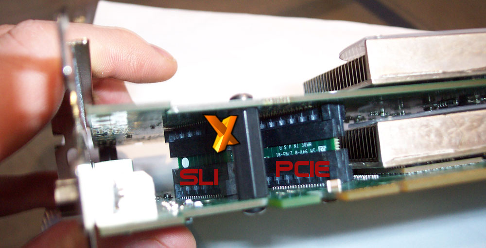
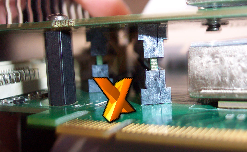
The extra communications logic is hard to see without screwdrivers, and I'd forgotten my cosh to incapacitate the board's owner while I attacked it with some watchmaker's drivers. My bad. You can see the post standoffs separating the two PCBs and the small PCBs doing the joining in the two slots. From a functional perspective, those connectors do block airflow from the primary/lower PCB on the board assembly.
Check out another view of the connector pair, here.
All this new hardware enables some new rendering modes. Time to go over those.


