BFG GeForce 7800 GS OC™
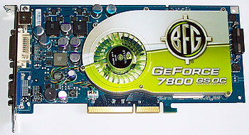
First thing to notice, and it's a not an obvious change from other 6 or 7-series parts, AGP or otherwise, is the analogue VGA connector is nearest the mainboard when installed, rather than at the top, and for reasons we can't quite fathom. Trace routing around the chip-to-BR2 link is likely less fun that way, too.
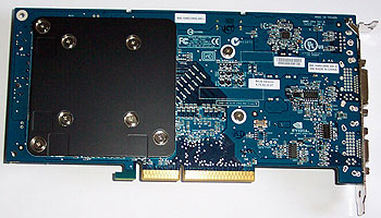
Also notice the AGP connector, heh, and the 4-pin Molex style power connector, rather than the 6-pin connector PCI express boards use. You can see right through to the PCB if you look at the fan, indicating the GPU is elsewhere. The rear of the board says yes to that.
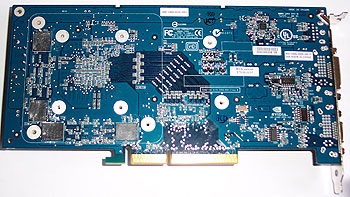
The recesses in the backplate tell you where the memory modules are and you can just about make out the (darker) traces running from AGP connector to somewhere under the backplate, letting you know the GPU is under there somewhere (but on the other side, obviously!). Let's prove that.
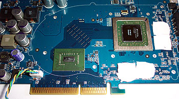
8 DRAM pieces make up the 256MiB compliment the board has, and you can clearly see how the GPU is routed to the BR2 and then to the AGP connector. The bridge is actively cooled by the board's heatsink, just like the G70 GPU is. An example packaged during week 34 (near the end of August) in 2005, the A2 revision of G70 on the BFG GeForce 7800 GS OC™ is physically the same chip as that on a GTX or GT on PCI Express.
Being an overclocked from the factory model, clocks on the BFG OC are 400/625, ahead of the reference clocks by 25MHz on both core and memory.
NVIDIA state the peak current draw at just over 6A from +12V. Any PSU worth its salt today will handle that with ease.


