


New technology
SMX - the glistening guts of Kepler
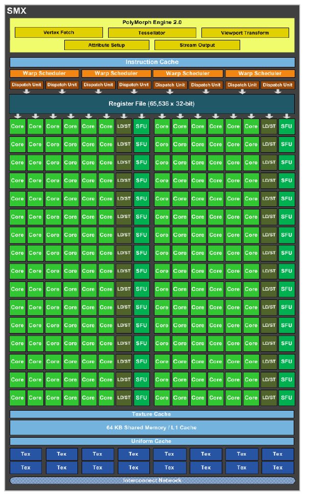
The SMX unit, of which there are eight in the full-fat GK104 Kepler, is where most of the calculations take place. The shading, be it pixel, vertex or geometry, is handled by the CUDA cores/shader-core units, the associated texturing is undertaken by the texture units at the bottom, and the load/store units go to-and-fro memory, saving and fetching data.
Lastly, the SFUs are special-purpose units that handle various maths such as transcendentals - something that the cores are not particularly good at. All in all, the topology is roughly analogous to Fermi.
One reason for having super-sized SMX units rests with efficiency. It is supposedly more efficient in terms of die real estate to have larger SM units, as you're not replicating as many setup engines over numerous units. NVIDIA could have chosen 16, rather than eight, per Fermi, but the aggregation of cores into fewer SM(X)s plays well for manufacturing purposes.
Going by the numbers, each of the eight SMs has 192 cores, 32 SFUs, 32 Load/Stores, 16 texture-units, one setup engine (PolyMorph 2.0), and four warp schedulers that can each dole out two 32-thread instructions per clock. This latter specification is double Fermi's, whose equivalent number of warp schedulers manage only one instruction per clock.
The NVIDIA-provided table, below, spells out the key differences in the various processing counts between the two architectures, taking the whole GPU into account.
Kepler isn't simply a blown-up version of Fermi, with everything multiplied by, say, 2x. NVIDIA has chosen to optimise the relationships between cores, texture units and schedulers, though, honestly, one needs to appreciate the part frequency plays before passing final judgement - just wait a while longer until we come to that.
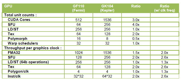
A peek at these Kepler figures, almost irrespective of frequency, because one can intimate it's good, would lead one to believe it's the Next Coming: 3x the core count, 2x the texture units, etc. However, it appears weaker in one key area. The PolyMorph Engine - NVIDIA-speak for the basic setup, including tessellation, before instructions get to the cores - is reduced from 16 to eight. NVIDIA says that the 2.0 variant, as found on Kepler, is able to deliver double the performance of the Fermi equivalent on a per-clock basis. Do your maths and a higher-clocked Kepler's setup is, on paper, faster than Fermi's, even though it has half the PolyMorph units.
Though you can't see it from the above table, Kepler has only 512KB of L2 cache, down from the 768KB on Fermi. NVIDIA still keeps the same 128KB per 64-bit memory controller architecture intact, so you can divine what's happened to the bus width before we spill the details. Less cache means fewer transistors, which is good for manufacturing, but not usually beneficial for performance. NVIDIA responds by saying that the L2 cache hit bandwidth - meaning the chances of actually getting the data you need in the cache - is now significantly higher in Kepler. Secondly, the speed of the cache is now increased, from 384 bytes per clock on Fermi to 512 bytes for Kepler. As the total bandwidth is also based on frequency, Kepler's is higher still (ed - don't give too much away on this page!)
NVIDIA is also at pains to establish Kepler as a gaming GPU in the first instance, but it picks up on some of the more GPGPU-orientated shenanigans present in Fermi. Kepler is much more productive at pushing through atomic operations, often used in multithreaded operations whose many threads may need access to the same data, and it's one pointer than the Kepler-based Quadro cards are very much in NVIDIA's thoughts.
We tried to find out whether, like Fermi, Kepler supports ECC memory, but NVIDIA stonewalled us, intimating that such details are to be disclosed when the HPC variant officially launches.
The Great CUDA makeover
You've probably got this far and have (at least) two questions: how can NVIDIA have 3x the core count when 512-core Fermi is already a massive GPU? Secondly, throwing this many cores, SFUs, and texture units into the mix must play havoc with the TDP; this has to be a 350W card? Let's answer the CUDA conundrum first.
Kepler does have 1,536 units, compared to Fermi's 512, but the cores are no longer clocked in at double the GPU's general clock. This is vitally important to understand. GeForce GTX 580 Fermi's cores operate at 1,544MHz while the bulk of the GPU itself runs at 772MHz. Kepler's operates at one speed. Now, it's actually more beneficial from a die-size point of view to operate with a shader 'hot clock,' per Fermi, because fewer, faster shaders take less space. This is precisely why the Tesla and Fermi cards adopt this approach; they don't have the die space to spare. Kepler, meanwhile, uses the same (lower) clock, and the main reason NVIDIA does this is to reduce power consumption.
You see, doubling the shader speed means the GPU consumes more power, but it's not as simple as that. Higher-clocked cores specifically need more pipelines stages that also each run at double the base clock: you have a compounded power-draw effect. Great for die area, bad for performance-per-watt.
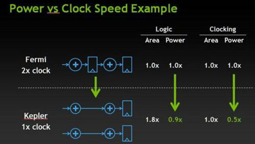
This picture illustrates this fact. Kepler uses more die space because it has more cores operating at base speed, but the removal of pipeline stages and associated power required for clocking means it has far nicer power-draw characteristics. It can be big and relatively cool.
The backend
We've learnt thus far that Kepler has wider, fatter SMX units whose cores operate at the GPU's base speed. NVIDIA's spent a significant part of its die real estate on these SMX units, so in order to keep manufacturing size to a minimum and reduce overall costs, hard decisions have to be made elsewhere.
Kepler throws out the die-expensive, power-hungry 384-bit memory bus of Fermi and replaces it with a fine-tuned 256-bit version. Now you're thinking something along the lines of 'how can all this SMX power be used with a itty-bitty 256-bit bus?' Fed from 32 ROPs - or one-third less than top-line Fermi - NVIDIA's use of a narrow-ish bus intimates that memory frequency is high. Kepler GK104 uses GDDR5 modules clocked in at 6Gbps, leading to overall GPU bandwidth of 192.3GB/s, or the same as Fermi.
Our feeling is that GK104 deserves a wider bus clocked just as high, solely due to how 'wide' it is at the upper portion of the chip, and, even with super-fast memory chips in situ, the GeForce GTX 680 may struggle at stupid-high resolutions and IQ settings. Another knock-on effect of a 256-bit bus is framebuffer size. Understanding that each card can use eight memory modules which connect to four 64-bit controllers, the choices are 1GB, 2GB, or 4GB. NVIDIA chooses 2GB, though partners may opt for 4GB on pre-overclocked models.
Architecture summary
Bringing it all together, Kepler is Fermi done right. It is designed to excel in one metric: performance per watt, and many of the design decisions allude to this thinking. Our one concern is with the 256-bit memory bus being swamped by the sheer grunt of the card, leading to sub-par performance with ultra-high resolution monitors or multiple-screen setups.


