Snip, snip, snip
GeForce GTX 480 and GTX 470 are both high-end desktop iterations of the GF100 architecture that we took a good look at on Friday. We encourage you to have a read and find out what makes them tick along.Shamelessly taking the specification-comparison table out of that review and pasting it below.
| Graphics cards | NVIDIA GeForce GTX 480 1,536MB | NVIDIA GeForce GTX 470 1,280MB | NVIDIA GeForce GTX 295 1,792MB | NVIDIA GeForce GTX 285 1,024MB | ATI Radeon HD 5970 2,048MB | ATI Radeon HD 5870 1,048MB | ATI Radeon HD 5850 1,024MB |
|---|---|---|---|---|---|---|---|
| General clock | 700MHz | 607MHz | 576MHz | 648MHz | 725MHz | 850MHz | 725MHz |
| Shader clock | 1,401MHz | 1,215MHz | 1,242MHz | 1,476MHz | 725MHz | 850MHz | 725MHz |
| Memory clock (effective) | 3,696MHz | 3,348MHz | 1,998MHz | 2,484MHz | 4,000MHz | 4,800MHz | 4,000MHz |
| Memory interface and size | 384-bit, 1,536MB GDDR5 | 320-bit, 1,280MB GDDR5 | 896-bit (2 x 448-bit), 1,792MB, GDDR3 | 512-bit, 1,024MB, GDDR3 | 512-bit (2 x 256-bit), 2,048MB | 256-bit, 1,024MB, GDDR5 | 256-bit, 1,024MB, GDDR5 |
| Memory bandwidth | 177.4GB/s | 133.9GB/s | 2 x 111.9GB/s | 159GB/s | 2 x 128GB/s | 153.6GB/s | 128GB/s |
| Manufacturing process | TSMC, 40nm | TSMC, 40nm | TSMC, 55nm | TSMC, 55nm | TSMC, 40nm | TSMC, 40nm | TSMC, 40nm |
| DirectX/ Shader Model | DX11, 5.0 | DX11, 5.0 | DX10, 4.0 | DX10, 4.0 | DX11, 5.0 | DX11, 5.0 | DX11, 5.0 |
| Vertex, fragment, geometry shading (shared) | 480 FP32 scalar ALUs, MADD + MUL | 448 FP32 scalar ALUs, MADD + MUL | 480 FP32 scalar ALUs, MADD + MUL | 240 FP32 scalar ALUs, MADD + MUL | 3,200 FP32 scalar ALUs, MADD + MUL | 1,600 FP32 scalar ALUs, MADD + MUL | 1,440 FP32 scalar ALUs, MADD + MUL |
| Single-precision GFLOPS (single-issue) | 1,345 | 1,088 | 1,192 |
708 |
4,176 | 2,720 |
2,088 |
| Texturing | 60ppc
bilinear 30ppc FP16 15ppc FP32 |
56ppc
bilinear 28ppc FP16 14ppc FP32 |
160ppc
bilinear 80ppc FP16 40ppc FP32 |
80ppc
bilinear 40ppc FP16 20ppc FP32 |
160ppc
bilinear 80ppc FP16 40ppc FP32 |
80ppc
bilinear 40ppc FP16 20ppc FP32 |
72ppc
bilinear 36ppc FP16 18ppc FP32 |
| ROPs | 48 |
40 |
56 |
32 |
64 | 32 |
32 |
| GPixels/s throughput | 33.6 |
24.28 |
32.26 |
20.74 |
46.4 |
27.2 | 23.2 |
| GTexel/s bilinear | 42 |
33.99 |
92.2 |
51.84 |
116 |
68 |
52.2 |
| Board power (max) | 250W | 215W | 289W | 183W | 294W | 188W | 170W |
| Multi-GPU | Three-way SLI | Three-way SLI | Two-way SLI | Three-way SLI | Two-way XFire | Four-way XFire | Four-way XFire |
| Board length | 10.5in | 9.5in | 10.5in | 10.5in | 12in | 11in | 9.5in |
| Connectors (native) | 2x
dual-link DVI Mini-HDMI |
2x
dual-link DVI Mini-HDMI |
2 x dual-link DVI, HDTV-out,HDMI | 2x
dual-link DVI HDTV-out |
2x
dual-link DVI Mini-DisplayPort |
2x
dual-link DVI HDMI, DisplayPort, |
2x
dual-link DVI HDMI, DisplayPort, |
| Etail price | £440+ | £299+ |
£350 |
£285 |
£550 | £310 | £225 |
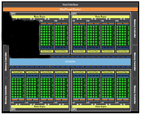
GeForce GTX 470 is differentiated and hamstrung when compared to GTX 480 in several ways. It loses what NVIDIA terms a stream-processing unit, composed of 32 cores, which bring the total count down from 480 to 448.
The SM units also carry four texture-unit blocks and, consequently, GTX 470's complement drops from a GPU-wide 60 to 56. The snip in architecture extends to the ROPs at the bottom, where one partition is deactivated. What's more, NVIDIA further reduces the GTX 470's potency by switching off a memory-controller partition, resulting in a 320-bit pathway. The loss in memory-bus width also results in removal of two memory chips, bringing the frame-buffer down from 1,536MB to 1,280MB, assuming same-density modules are used. Last, but not least, the clock-speeds see a downward bump across the board.
NVIDIA's GF100 uses a big, expensive die. Any GPU that doesn't make the GTX 480 grade - and we suspect that to be many in the initial runs at TSMC - is binned, hopefully, at GTX 470 grade. What this means is that it's still the 3bn-transistor GPU which has proven rather difficult to cool.
The numbers tell us that GTX 470 will have difficulty in matching the peak power of the Radeon HD 5870 GPU, yet we don't think NVIDIA can make a huge loss by selling the GPUs and memory to their partners at a cost low enough to compete with the Radeon HD 5850's street price of £225, including VAT.

In an altered block diagram which the author's five-year-old niece could have done a better job on, here's how GTX 470 stacks up against the ideal GF100 architecture, based on a 512-core design. It's not quite that simple, of course, but you get the idea....


