RV770. What is it all about
Background
Let's make one aspect clear from the outset. ATI is not competing with NVIDIA at the high-end of the GPU market. It can't, just like AMD cannot go toe-to-toe with Intel's fastest quad-core CPUs. NVIDIA will retain the ultimate performance crown for a while yet.ATI's engineers realised this after the much-delayed launch of R600 - Radeon HD 2900 XT - and, ever since, executive after executive has been vigorously beating on the value drum - that is, when they're not busy leaving for, dare we say, greener pastures.
Two new GPUs are being announced today. Going under the code-name of RV770, the Radeon HD 4850 and HD 4870 will be priced at $199 (£125) and $299 (£175), respectively. They need to offer compelling reasons for eschewing a range of strong mid-range performers from NVIDIA - GeForce 8800 GT (£99), 8800 GTS 512 (£139); 9600 GT (£89); and 9800 GTX (£175) - and, funnily enough, from ATI's own stable, in the form of the price-ravaged Radeon HD 3850 (£79) and 3870 (£89).
The two GPUs are differentiated solely on the basis of speeds, with the Radeon HD 4870 using faster core clocks and significantly faster memory, via GDDR5.
RV770 demystified?
What's the same?RV770 began life around 30 months ago from a design standpoint, according to co-lead architect Eric Demers. Teams from Shanghai, Toronto, and Orlando worked on the architecture, cleaning up ill-fated R600 and focussing on both gaming and stream (GPGPU) performance. Demers further commented that performance-per-watt and performance-per-dollar were the key driving characteristics of RV770.
Getting the menial portions out of the way first, RV770 supports Radeon HD 3800-series' entire feature-set, including DirectX 10.1/SM 4.1; SIMD processing arrays; 55nm fabrication; PCIe 2.0 interconnect; on-board tesselator; second-generation Avivo; power management in the form of Power Play; and CrossFireX multi-GPU technology.
The unified architecture's stream processors still operate at the GPU's core speed, unlike NVIDIA GPUs' clear split-clock domain, and ATI's kept a 256-bit memory bus from the on-board frame-buffer to the raster back-ends and caches.
What ATI has done, in comparison to RV670, is put shading capability - facilitated by DX10 - and texturing speed very much to the fore.

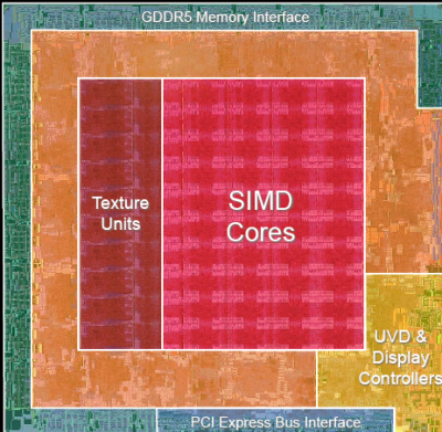
Reinforcing that fact is the space taken up by both shading (SIMD cores) and texturing on the die. Between them, they take up over half of what's available.
RV770 can do everything RV670 can, only faster, so let's discover how.
A little history, and now more horsepower and efficiency
Radeon HD 3870 leverages 64 clusters that each hold five stream processors; one of which is tasked with additional computational work. Thinking of it in terms of throughput, each stream processor - which can work on either vertex, pixel, or geometry data - is able to process and spit out both a multiply and add instruction (MADD) at the same time. Adding it up, HD 3870 offered almost 500 GFLOPS of potential throughput (64x5x2x775).
The design is a little lopsided in that texturing, the next part of the rendering equation, isn't quite as prolific. The GPU can texture-address and bilinear-filter (INT8) and FP16-type-filter - usually for high-dynamic range lighting - 16 pixels per clock.
As a comparison, GeForce 8800 GT 512 can bilinear-filter 56ppc and FP16-filter 28ppc, at roughly equivalent core speeds to the Radeons. Why is this important, you may ask? The ability to slap texture(s) on a calculated shape, usually a polygon, means that it looks more life-like - it literally has texture. The texture-filtering speed is important because it defines how the texels will be colour-merged to provide the final pixel colour - what you see on the screen.
Coming down a bit further, 16 render back-ends, grouped in blocks of four, then take all this processing, helped by the storage space that's card-mounted memory, and apply post-effects, such as antialiasing. The final, refulgent output is drawn on to your screen
ATI's Radeon HD 3800-series, strong in most areas, lacks finesse when running with antialiasing; the performance drop-off when compared to non-AA usage is significant, and with image-quality very much to the fore, ATI suffers when compared to NVIDIA's more-efficient mid-range implementation.
The upshot is that significant shading power (496GFLOPS) is somewhat hamstrung by a relatively low texel fillrate (12.4Gtexel/s) and poor antialiasing performance. Phew, got all that?
Architecture comparison
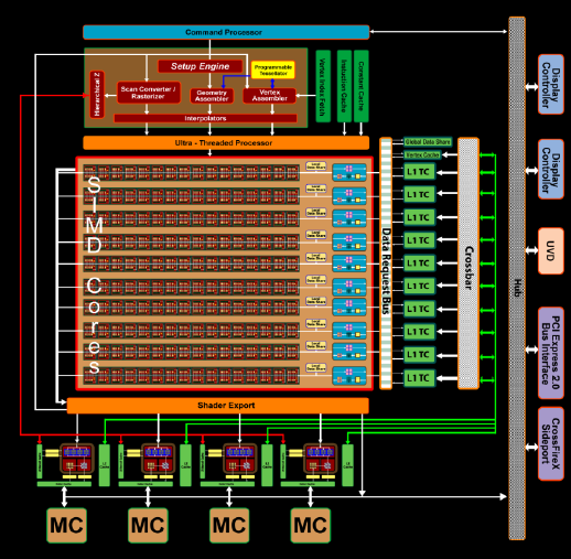
Much like NVIDIA's recent introduction, RV770 has its roots firmly entrenched in the previous generation's architecture. Harnessing the ever-so-useful block diagram:

Take a look back at the Radeon HD 3870's block diagram, here, to see the difference.
There's a lot more of, well, everything in RV770, yet the die size, based on the now-established 55nm process, has gone up from 192mm to just 260mm - or less than half the size of NVIDIA's GTX 200-series. We'll explain how and why in the process of the discourse.
Now, the two diagrams aren't that different in basic setup. The command processor, setup engine and ultra-threaded dispatch processor are at the top. Their job is to organise and push thousands of concurrent threads - be they pixel, vertex, or geometry - to the SIMD (shader) array that dominates the middle of the diagram.

Shade me silly
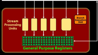
Taking a closer look at those teeny-weeny squares, prima facie, there's a change in SIMD deployment. RV770 may employ the same SIMD-based arrangement as RV670, meaning five stream processors and a branch execution unit, but the differences are in how they're laid out and communicate with one another and, of course, amount.. Whereas RV670 grouped 64 together for a total of 320 SPs, RV770 pulls together 160 of these SIMDs, grouped in 10 cores of 16, which total 800 SPs (10x16x5), or, putting it another way, 250 per cent higher than the previous generation.
Each 32-bit floating-point, scalar SP can be set to work on any thread and in single-precision mode issue two instructions per clock. Ramping it up to double-precision (64-bit), the architecture doesn't support it natively. Rather, it has to use its 32-bit SPs, run over a number of cycles that aggregate output, but ATI reckons RV770 is still good for one-fifth of single-precision throughput. That's a lot of FLOPS, and we'll come back to this later.
Coming back to deployment, every core's SIMDs are fed by their own instruction set. The SIMDs can now use the calculations of another SIMD, in the same core, to better-improve overall performance, thanks to the per-core 16KiB cache - sat between the SPs and texture units. As the name suggests, it's a local store that all SIMDs have access to, thus keeping everything ticking along at near-100 per cent efficiency. A separate global data cache, accessed by the data request bus, helps keep GPU-wide SIMDs in order, too.
How has ATI managed to include 800 SPs - an increase of 250 per cent over RV670 - with a die-size increase of 'only' 35 per cent? Each SP has undergone a rigorous diet, for 40 per cent less die space. ATI wouldn't divulge details of just how this crash diet was achieved without performance compromise.
The SPs are now more efficient in a couple of ways. Firstly, they now have granular clock-gating technology, which means that SPs can be turned to idle when no work is occurring and switched to full-active mode, quicker, when there's work to be done. Secondly, they include what's termed integer bit shift operations, useful for video processing - transcoding in particular - and fixed-point-type processing, and ATI reckons the RV770 architecture is some 12.5x faster than RV670 in this respect.


