A new generation of Intel processors
The annual Consumer Electronics Show (CES) held at the turn of the year in Las Vegas, Nevada, is usually the place to be for important technology launches.
12 months ago, Intel used the pretext of CES to launch the 2010 Core Processor family for both mobile and desktop platforms. The chip giant separated branding into three muddled categories - Core i3, Core i5 and Core i7 - and paid particular focus to new chips with integrated graphics.
This year, the chip giant is bolstering its mainstream CPU line-up with a second-generation Core Processor family that promises to bring eye candy to the masses.
Second-generation mojo
Based on a new architecture known as Sandy Bridge, Intel's Core 2011 range is exclusively hewn from 32nm silicon and promises energy-efficient performance, a finer implementation of Turbo Boost, improvements in the integrated graphics' abilities, and other desirable add-ons.
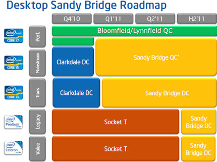
Before we get into specifics, here's a general overview of how Intel sees Sandy Bridge chips grabbing the mid-range baton from incumbent Clarkdale CPUs and running away with it for the remainder of 2011. Sandy Bridge will quite clearly provide the bulk of Intel's chip revenue this year, leaving little room for the high-end LGA1156 and LGA1366 Core i7 chips, as represented by the thin green line.
'Free graphics'
It's kind of unfair to label Sandy Bridge processors as CPUs, frankly. Every single chip in the range features integrated graphics that are part of the same silicon used to produce the traditional CPU cores. There's simply no getting around the fact that buying into Sandy Bridge - be it for desktop or mobile - means having some level of graphics ability thrown in. Whether you see it as free or an unnecessary expense depends entirely upon your viewpoint.
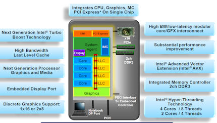
This high-level overview depicts the Sandy Bridge architecture. The monolithic piece of silicon represents the top-level chip, and Intel differentiates between Sandy Bridge processors through four main factors: CPU cores, clockspeed, hyperthreading support, and graphics cores.
Core iBlimey
The optimum chip comprises of a 3.4GHz four-core, eight-threaded CPU section that's backed up by a graphics segment home to 12 execution cores - phew! Run down to the runt of the litter - read cheapest - and Sandy Bridge, on the desktop, can consist of a 3.1GHz, two-core, four-threaded chip with six execution units for graphics. Got all that?
What you need to takeaway here, folks, is that Intel can split the modular core architecture in many different ways, and this bifurcation is what leads to chips being pushed into Core i3, Core i5, or Core i7 divisions.
Making Sandy Bridge the generation divide
Before we make your head spin with the plethora of retail options it's prudent to explain what makes Sandy Bridge different to the 2010 range of Core processors.
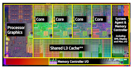
First off, let's remember that you're looking at a single piece of silicon for all the computational duties, be they graphics or CPU. This juxtaposes with the two-chip approach taken on the Core 2010 chips. The silicon is based on Intel's 32nm, high-k metal gate technology and the small transistor size enables the chip giant to produce the full-fat Sandy Bridge - four cores, eight threads, fast graphics - with a die size of around 216mm².
Truly shared cache
The chips keep the 64KB L1 and 256KB L2 cache per core arrangement found on 2010's Clarkdale CPUs and also carry over the last-level cache (LLC, aka L3 cache) which varies in size, between 4MB and 8MB, depending upon specific Sandy Bridge model. This LLC plays a dual role for Sandy Bridge, as it's the go-to cache for both the CPU cores and integrated graphics. Given a situation of concurrent CPU and GPU load, with both portions of the chip screaming for LLC bandwidth, Intel maintains that Sandy Bridge's graphics driver determines just how much of the LLC is apportioned to the GPU.
Actually, look closer and the LLC is tied to the CPU cores, graphics, system agent and media processor by a four-ring interconnect that is borrowed from the high-end 'EX' parts. It's needed to keep all the bandwidth-sucking parts of the CPU within easy reach of the large on-chip cache, which now operates at the same speed as the CPU cores.
Tying it together
Sandy Bridge harnesses the foundations of last-generation Clarkdale by using an integrated memory controller, connecting through a dual-channel DDR3 memory controller, and DMI interface to a southbridge chip.
All processors have a built-in PCIe controller, too, which provides support for external, discrete graphics by way of a x16 link that can be split into two x8 for either AMD's CrossFire or NVIDIA's SLI GPUs.
Keeping it modern, the chip houses what Intel terms the 'System Agent'. A fancy term for the part of the processor that handles display duties and menial processing tasks - kind of like the uncore portion of existing Intel chips. Look inside that bit of silicon and Intel crams in a DisplayPort controller. Whether board manufacturers take it up will depend upon their implementation.
You may be reading this and thinking that there's not a huge improvement here, save for the one-chip silicon, but the devil, as always, is in the detail. Let us explain on the following page.


